Overview
Designed a two-stage operational amplifier to drive a 10-bit DAC display load (1 kΩ ‖ 25 pF) with a closed-loop gain of 2 V/V, ≤0.2% settling error, and ≤180 ns settling time for a 1.4 V step. The architecture is a telescopic cascoded differential first stage driving a source-follower buffer and a Class AB output stage biased with a Monticello network for mismatch robustness.
System-level sizing started from a MATLAB script that derived gm1, gm2, and the gain split from the settling-time, phase-margin, and error specifications. Transistor sizing was then iterated using the gm/Id methodology in Virtuoso.
What I did
- Topology selection: chose telescopic cascode + source-follower + Class AB output to meet gain and output-swing requirements within the 1.8 V supply.
- System-level design: wrote a MATLAB script to compute required transconductances, compensation capacitor sizing, and per-stage gain from the spec sheet (target loop unity-gain frequency, phase margin, dynamic error).
- Transistor sizing: applied gm/Id sizing for each device using 2 V devices (the supply is VDDH), then iterated DC operating points and W/L sweeps to converge to the operating region.
- Compensation: sized the Miller capacitor to bring phase margin as close to 45° as possible while meeting settling.
- Mismatch robustness: selected the Monticello biasing scheme for the AB output stage to reduce sensitivity to Vth and mobility variation.
- Verification: ran AC (loop gain, CMRR, PSRR), transient (settling, error, supply current), and load-dependence simulations across 0.75 kΩ and 1 kΩ loads.
Results
| Specification | Requirement | Measured (0.75 kΩ) | Measured (1 kΩ) |
|---|---|---|---|
| Closed-loop gain | 2 V/V | 2 V/V | 2 V/V |
| Settling time | ≤ 180 ns | 164 ns / 132 ns | 177 ns / 173 ns |
| Total error | ≤ 0.2% | ≤ 0.2% | ≤ 0.2% |
| CMRR @ DC | ≥ 55 dB | 78.06 dB | 78.06 dB |
| PSRR @ DC | ≥ 50 dB | 68.33 dB | 68.33 dB |
| Phase margin | ≥ 45° | 47.94° | 48.45° |
| Output swing | ≥ 1.4 V | 1.4 V | 1.4 V |
| Power | ≤ 0.75 mW | 0.84 mW | 0.90 mW |
All specifications met except the stricter EE 240A power budget (came in 12–20% over). The miss is attributable to bias-current sizing in the output stage; reducing the AB stage quiescent current would close the gap at some cost to slew rate.
Approach and key decisions
Why telescopic over folded cascode. Telescopic gives higher gain at lower power than folded cascode, at the cost of reduced output swing. Since the second-stage source follower handles the output swing requirement, the telescopic was the right trade for the gain budget.
Why a source-follower buffer between stages. Maintains high output impedance of the first stage (preserving gain) while presenting low impedance to the AB output stage gates.
System-level script first, hand-sizing second. Doing the algebra in MATLAB first, computing gm1 = ω_ol · Cc and gm2 from the closed-loop bandwidth, error, and phase-margin targets, meant the Virtuoso iteration started from a known-feasible point rather than guessing.
Power miss honest accounting. The output stage bias was tuned for fast settling under the worst-case load. Hitting the 0.75 mW spec is achievable but requires re-tuning the Monticello bias and likely accepting tighter settling margin.
Figures
Design
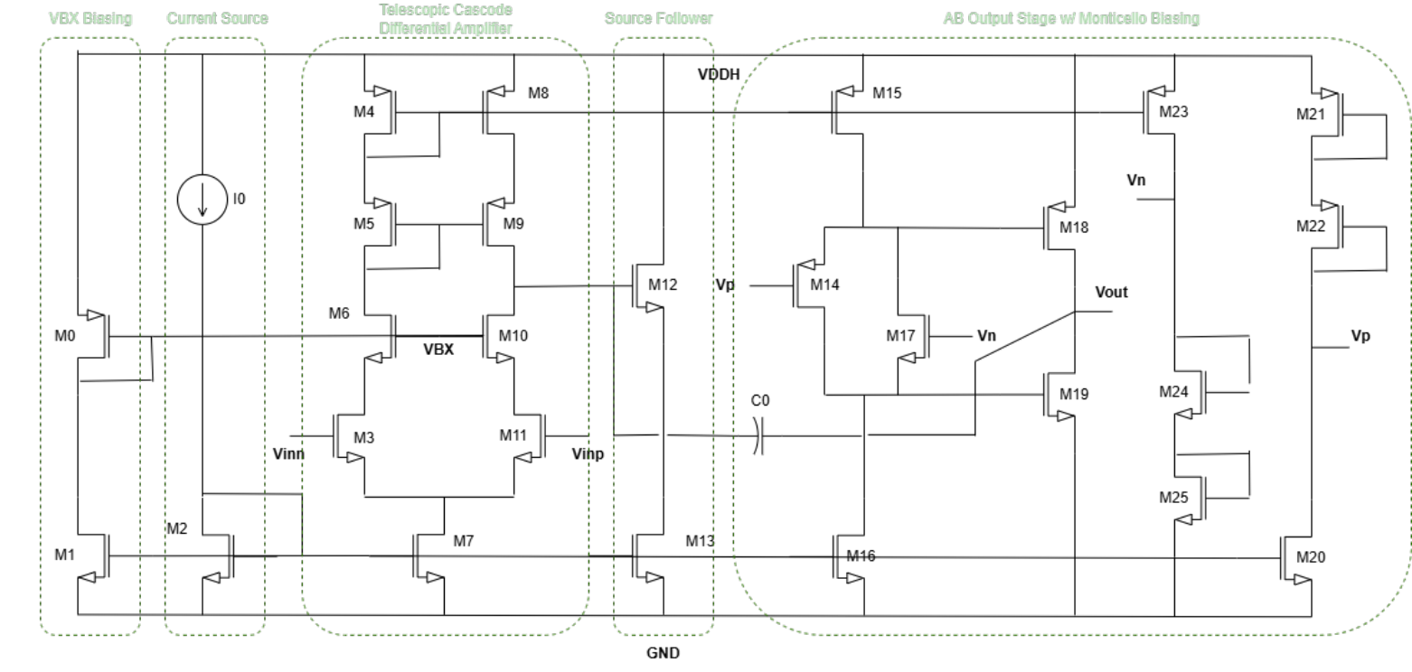 Full transistor-level schematic, annotated by stage (report Fig. 1).
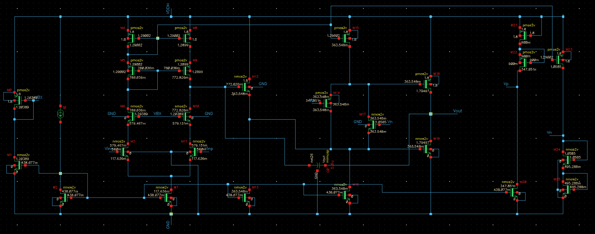 The same amplifier captured in Cadence Virtuoso (report Fig. 2).
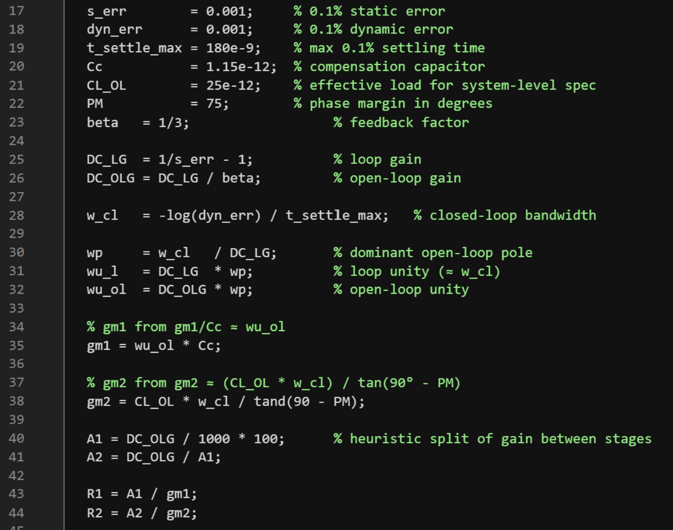 MATLAB system-level design script: the spec-driven sizing done before Virtuoso iteration (report Fig. 3).
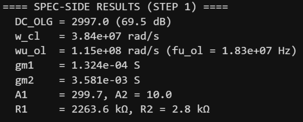 Script output: DC_OLG = 2997 (69.5 dB), gm1 = 132 µS, gm2 = 3.58 mS, A1 = 299.7, A2 = 10.0 (report Fig. 4).
Simulation results
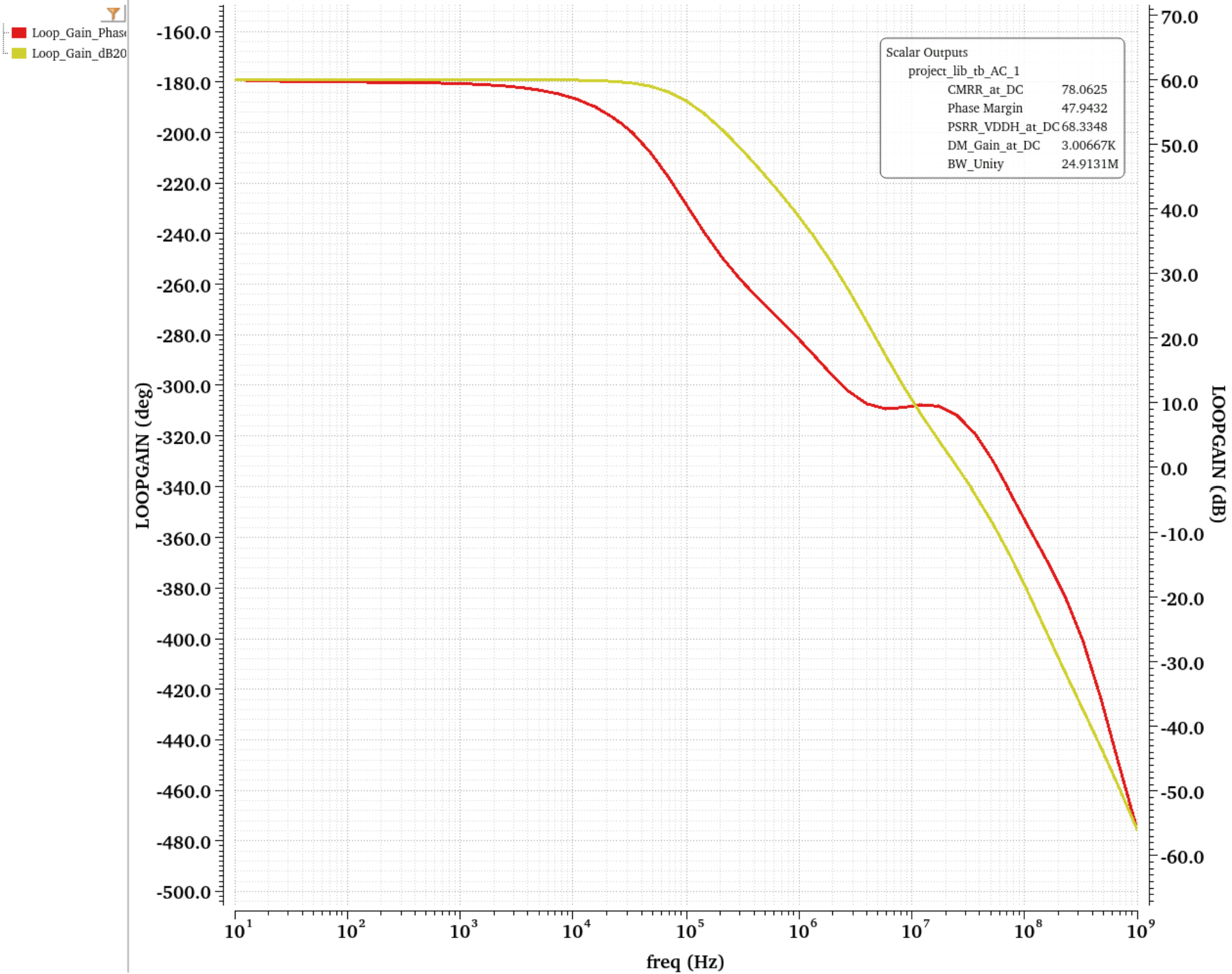 Loop-gain Bode plot, 0.75 kΩ load: phase margin 47.9°, CMRR 78.1 dB, PSRR 68.3 dB, unity-gain BW 24.9 MHz (report Fig. 5).
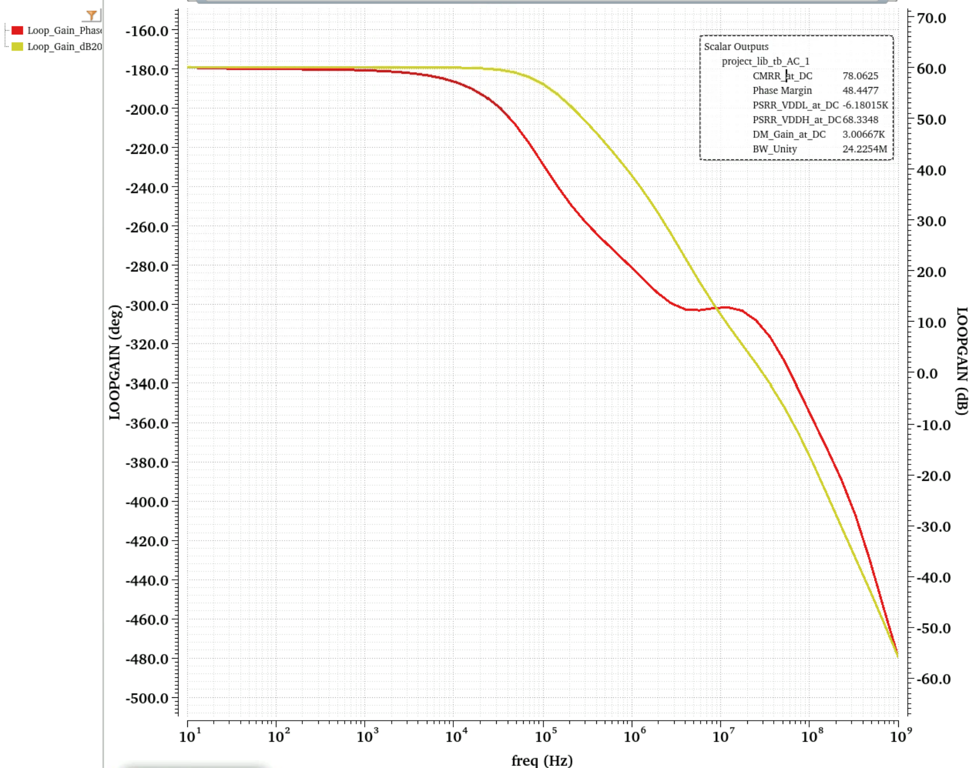 Loop-gain Bode plot, 1 kΩ load: phase margin 48.5° (report Fig. 6).
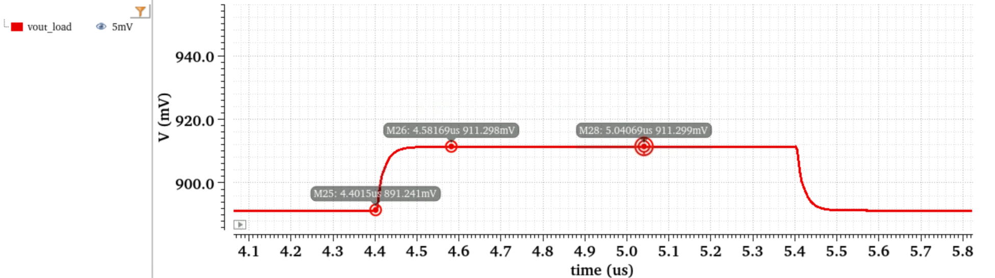 Transient settling of the load-capacitor output to within 5 mV (report Fig. 13).