Overview
A hardware–software co-designed compressed ultrasound imaging system that reconstructs a sparse 3D scene from only eight PMUT (piezoelectric micromachined ultrasonic transducer) sensors, rather than the hundreds typically required. By driving the array with optimized, mutually-incoherent transmission profiles and pairing it with a physics-based forward model and GPU-accelerated reconstruction, the system images a 1 m × 1 m × 1 m field of view.
This was a six-person M.Eng capstone in the Liwei Lin Lab. My contribution was the PCB implementation: the single 6-layer mixed-signal PCB that drives the PMUTs, captures their echoes, and streams digitized data to the host. The control firmware, PMUT characterization, forward model (k-Wave), and FISTA reconstruction were handled by other team members.
Mentorship: I mentored an undergraduate researcher in PCB design throughout this project — guiding them through schematic capture, layout, and board bring-up.
What I did
- Transmit path: designed the high-voltage pulser front end (TC4427 MOSFET drivers + HV2707 analog switch) generating the 15 V drive pulses that excite the PMUTs at resonance.
- Receive path: VCA5807 low-noise variable-gain amplifier feeding an AD7606C-18 18-bit, 8-channel simultaneous-sampling ADC, with a TR-switch isolating the sensitive receive front end from the high-voltage transmit pulses.
- Power management: LM2733 boost and LM27761 charge-pump converters for the bipolar/high-voltage rails, with a TPS22918 load switch for controlled power sequencing.
- 6-layer mixed-signal layout: stackup partitioned as top analog signal / analog ground / analog power / digital power / digital ground / bottom digital signal, with separated analog and digital grounds to keep high-speed digital switching noise out of the low-amplitude analog echo path.
- Board bring-up: validated power delivery, the ICs, and end-to-end system functionality with an oscilloscope, signal generator, and multimeter.
Results
| Metric | Value |
|---|---|
| Sensors | 8 PMUTs on a single board (75 mm × 50 mm aperture) |
| PCB | 6-layer mixed-signal, fabricated and assembled |
| Acquisition | 18-bit, 8-channel simultaneous sampling |
| Transmit drive | 15 Vpp HV pulses at PMUT resonance |
| Reconstruction field of view | 1 m × 1 m × 1 m (22,321-voxel grid) |
Approach and key decisions
Co-design instead of brute force. The defining choice was to make eight sensors do the work of hundreds. Both the array layout and the transmission frequency/delay profiles are optimized for low mutual coherence (using a Gram-matrix metric, L-BFGS-B with multiple restarts), so each acquisition yields maximally distinguishable measurements, the prerequisite for sparse compressed-sensing reconstruction. The hardware exists to make those diverse measurements cleanly.
Mixed-signal discipline drove the PCB. With 15 V switching pulsers sitting next to a microvolt-scale receive front end on one board, signal integrity was the hard constraint. The split-plane, split-ground 6-layer stackup is what keeps the digital and high-voltage switching currents from contaminating the analog echo path the ADC has to read.
Hardware-discretized optimization. Optimized transmission frequencies (40–60 kHz, 2 kHz steps) and delays (0–200 µs, 10 µs steps) were projected onto the grid the Teensy can actually produce, so the optimizer’s output is directly implementable rather than theoretical.
Figures
System
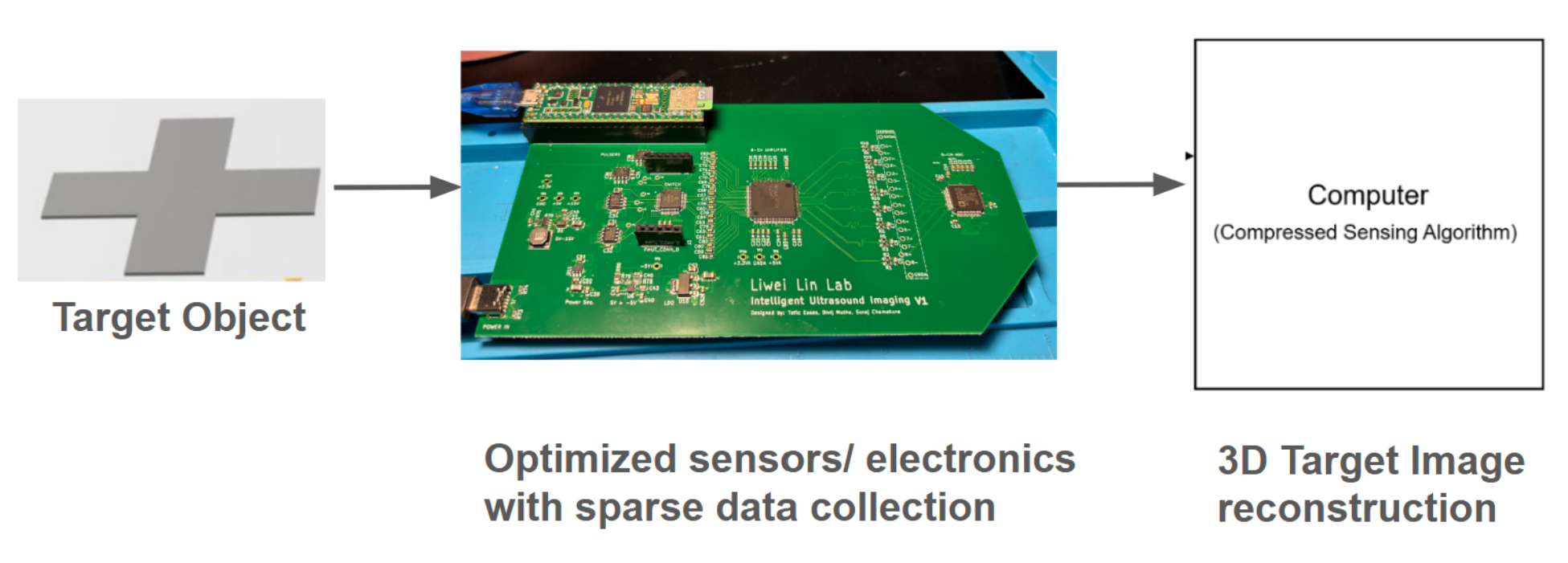 End-to-end system: target, optimized sparse-sensor electronics, then 3D reconstruction (report Fig. 1).
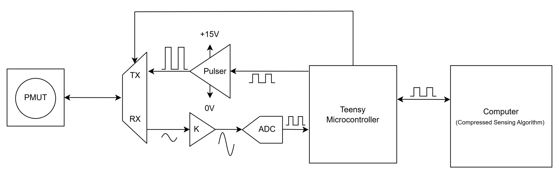 Electronic system diagram: transmit (pulsers) and receive (amplifier into ADC) pipelines (report Fig. 2).
Schematics
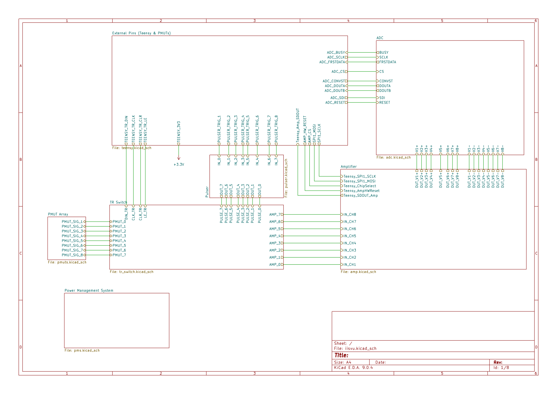 Top schematic: each sub-sheet is one subsystem of the electronic system (report Fig. 3).
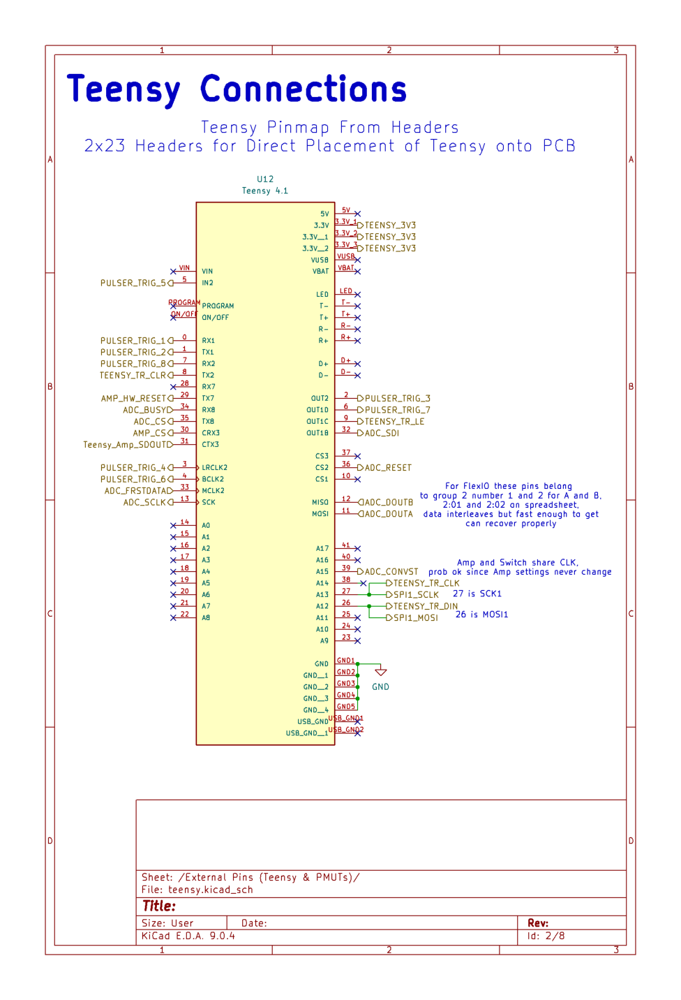 Teensy 4.1 controller sub-sheet (report Fig. 4).
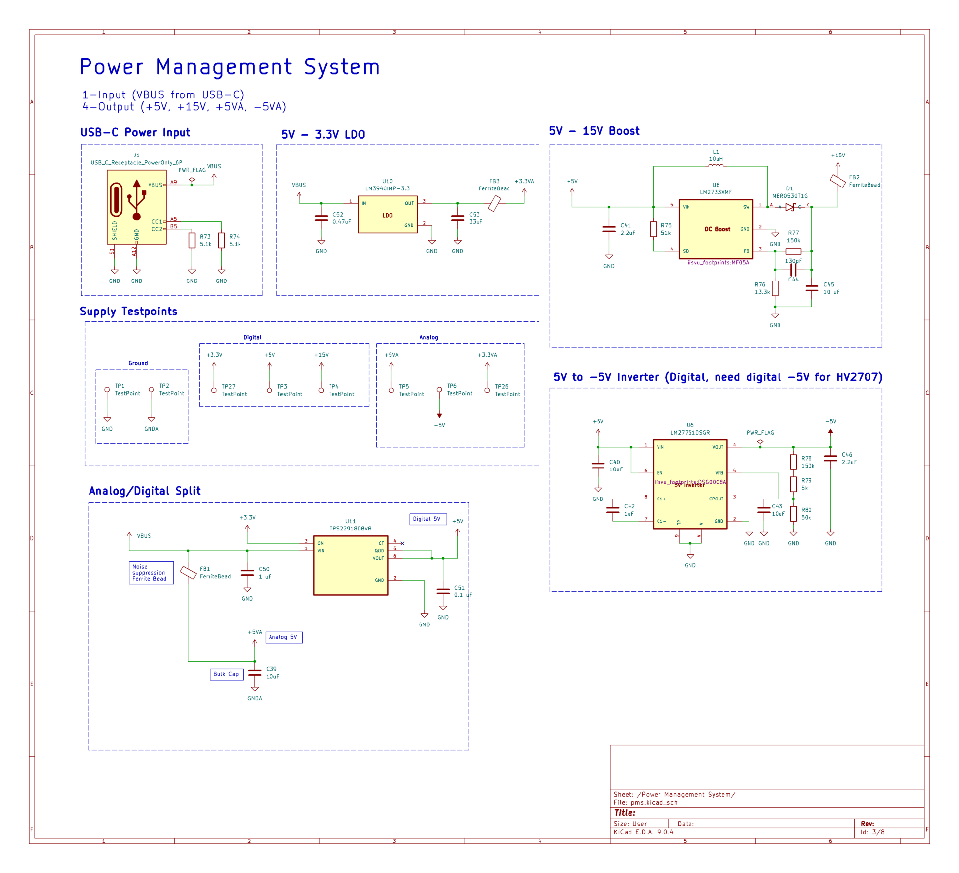 Power management: boost and charge-pump rails with sequencing (report Fig. 5).
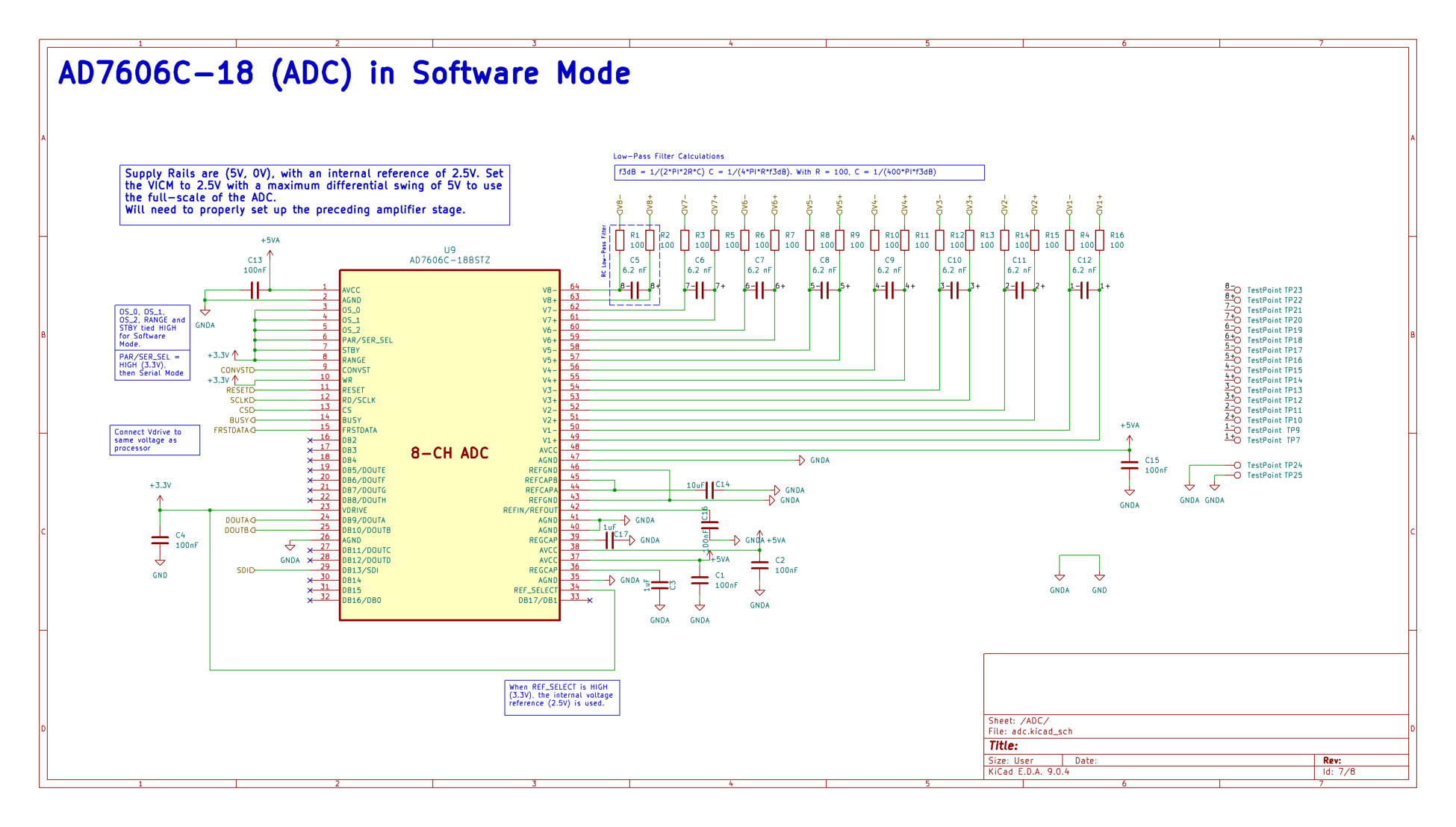 AD7606C-18 8-channel simultaneous-sampling ADC (report Fig. 6).
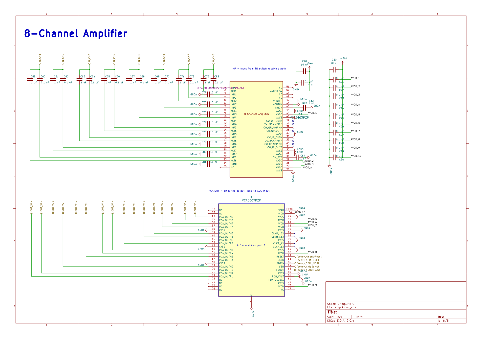 VCA5807 low-noise variable-gain receive amplifier (report Fig. 7).
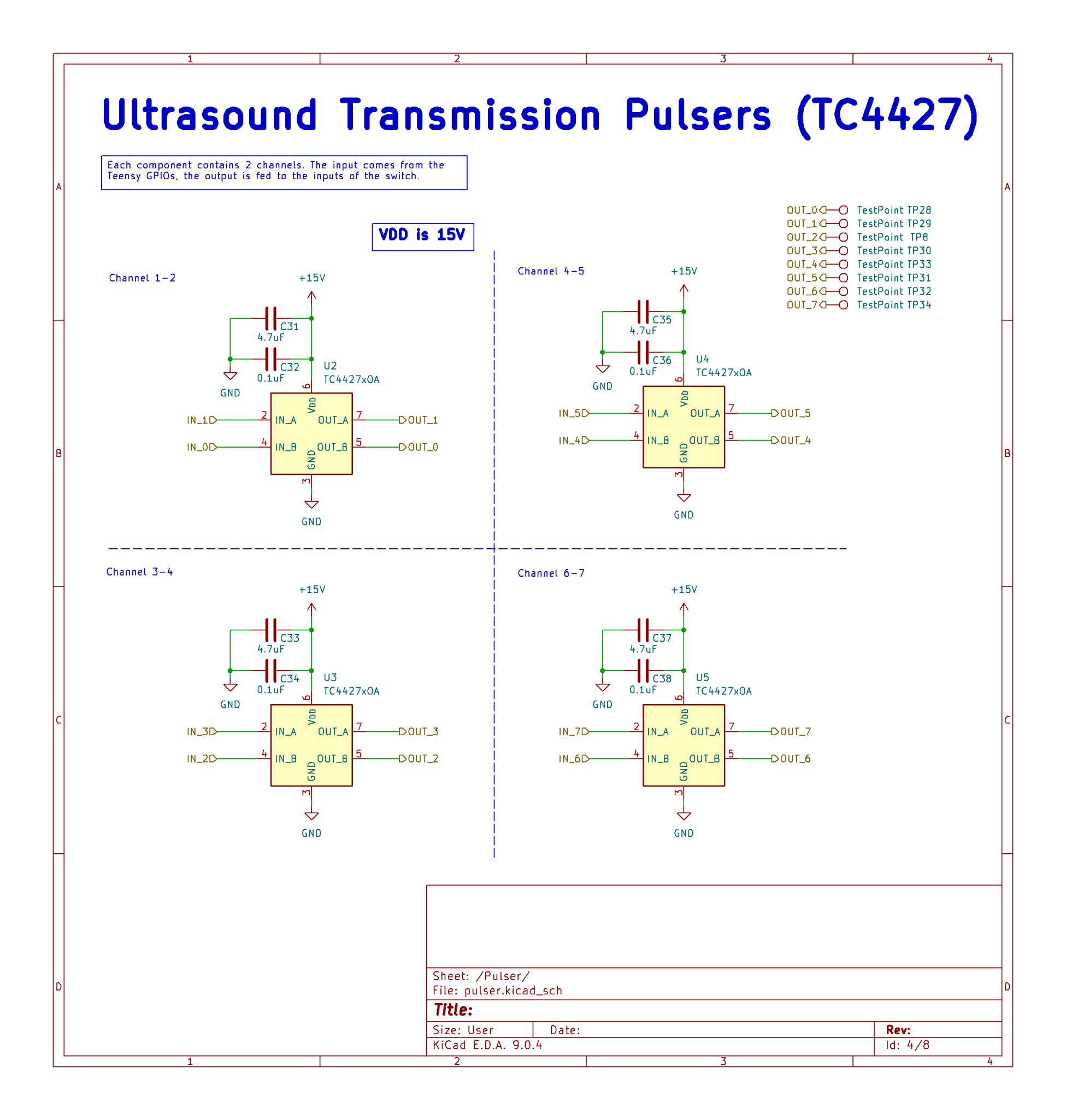 High-voltage transmit pulsers (TC4427 drivers) (report Fig. 8).
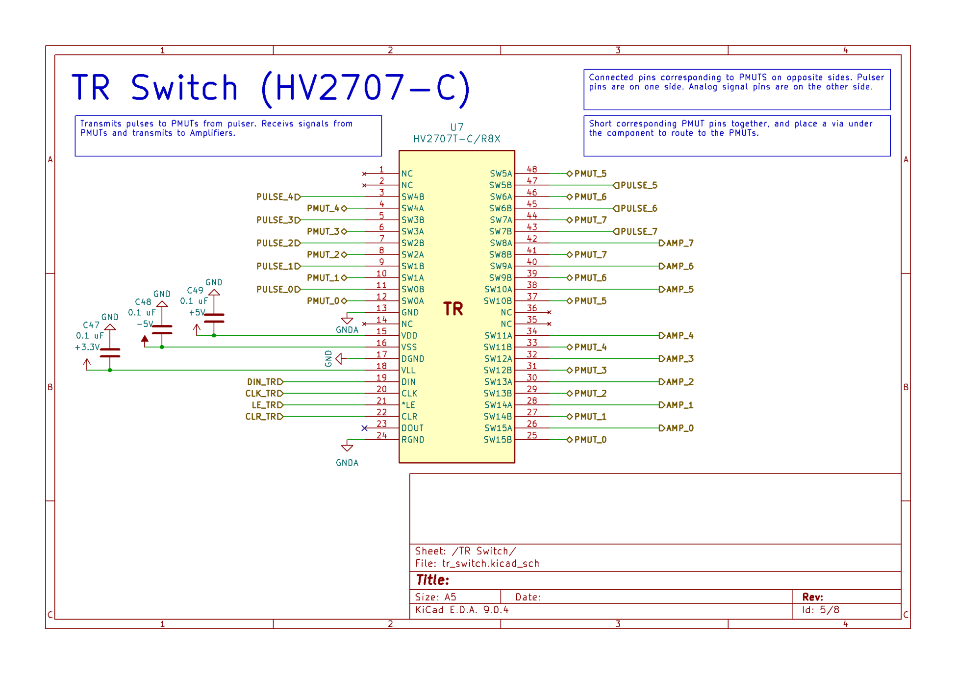
 TR-switch (HV2707) isolating the receive front end from the HV pulses (report Fig. 9).
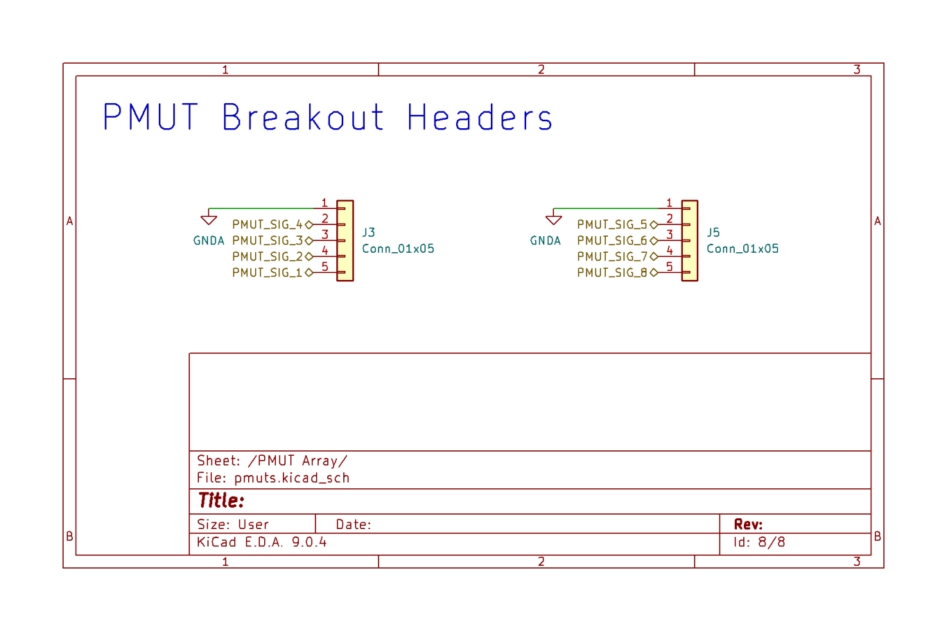
 PMUT array breakout headers (report Fig. 10).
PCB
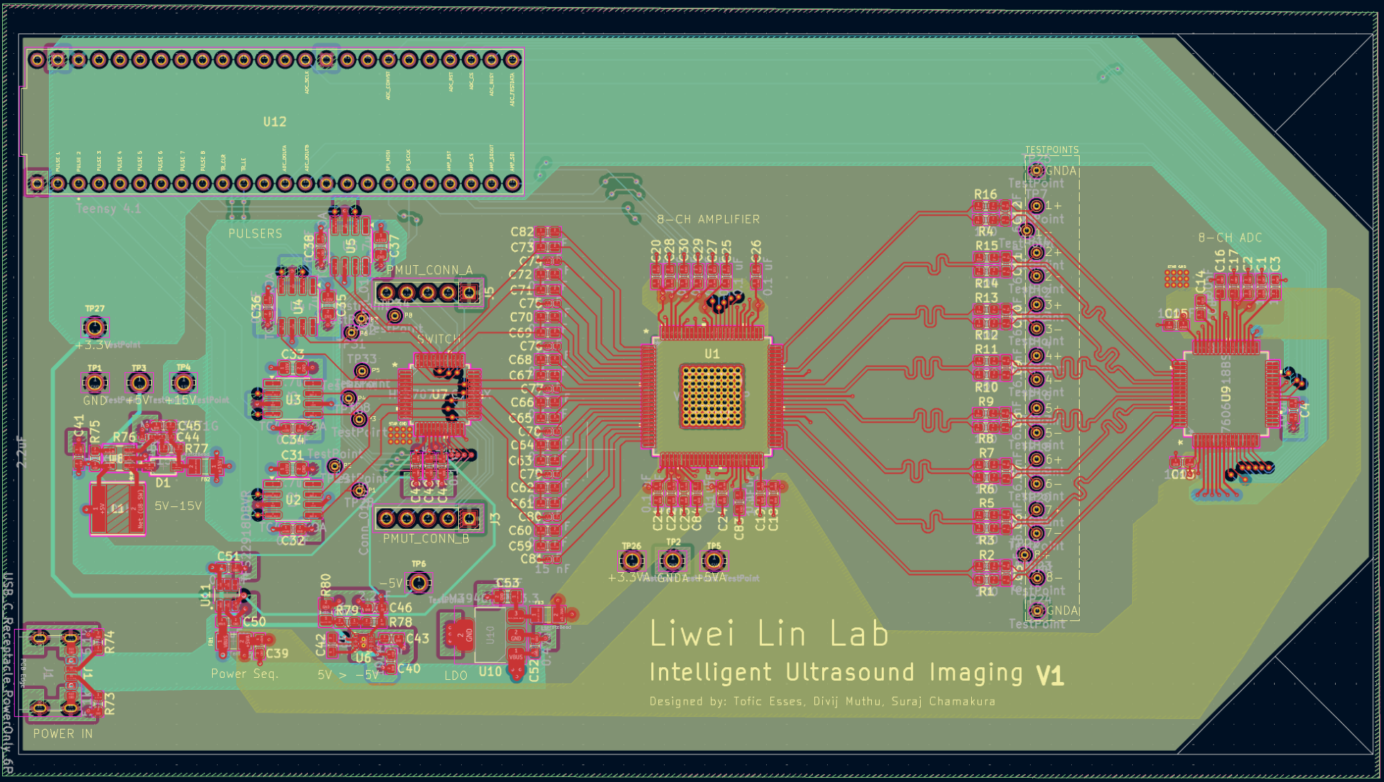 6-layer mixed-signal PCB layout with partitioned analog/digital planes (report Fig. 11).
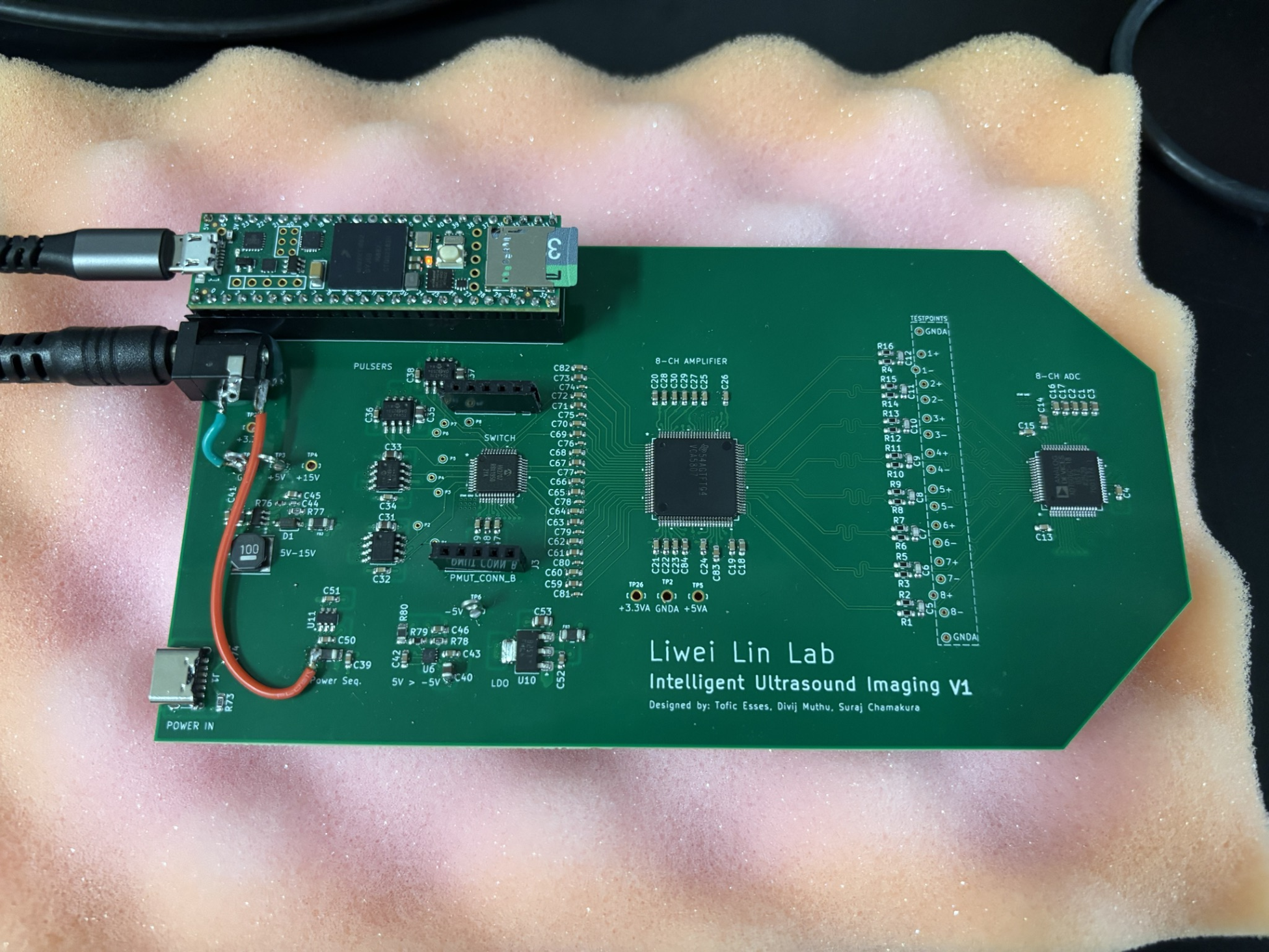 Assembled board: physical realization after fabrication and assembly (report Fig. 12).