Overview
A capstone project at EngerLab to design a cost-efficient, modular, multi-channel scintillation detector for automated PET radiopharmaceutical synthesis. Positron-emission-tomography scans require patients to take radiopharmaceuticals, which must be synthesized and validated using scintillation detectors, and existing detectors are expensive, bulky, and non-modular. Scintillating materials emit photons when exposed to radiation; those photons can be measured and quantized for real-time monitoring.
This was a multi-disciplinary team of six, two Medical Physics PhD students and four engineers (EE/CE/SE). My role: the only firmware developer, the 3D-enclosure designer, and one of two hardware designers, which gave me a large influence on the project’s scope and direction and required constant coordination with the software engineer for firmware–application integration.
What I did
- Firmware (C++): got two ESP32s (a Leader and a Follower) sampling concurrently and enabled multi-channel connectivity for modularity. I modeled the behavior as a state machine before writing code, with ESP-NOW point-to-point wireless carrying the inter-MCU communication at each state transition.
- Data/command protocol: a DATA TABLE formatted by the RX/TX module carries readings from multiple detector channels up to the application, and a COMMANDS TABLE formatted by the application distributes commands back down to each channel.
- Hardware: designed the compact RX/TX module PCB first, then the Signal Acquisition Module (SiPM devices, capacitors holding a stable 29.4 V bias, current-limiting resistors, in a fully light-tight enclosure), and contributed to the Detector Module main PCB: raw-signal processing (amplification, peak detection, buffering), a DC-DC boost from 5 V to 29.4 V for SiPM biasing, and the dual ESP32s. Circuits were simulated in LTspice before layout.
- Enclosure: designed the 3D-printed enclosure in Fusion 360 so detectors stack like Lego blocks, with vertical power connectors distributing power across modules from a single adapter.
Results
The detector was set up with optical-fiber cables feeding the Signal Acquisition Module input; behind a lead wall sat a scintillating spiral-fiber holder loaded with a low-activity radioactive source. Readings displayed on the application were largely constant, the expected result for a low-activity source.
Honest scope: the team did not fully complete the system (a calibration feature was planned but cut for time, so the result plot is raw data only). The progress made was pivotal to the device’s development and is continuable thanks to extensive documentation.
Approach and key decisions
State machine before code. Two MCUs sampling concurrently and exchanging data over wireless is exactly the kind of system that goes wrong if you start coding before modeling it. Drawing the Leader/Follower state diagrams and the per-transition ESP-NOW message exchange first is what made the concurrency correct.
Build small first. I completed the small RX/TX module before the larger boards, so the communication and packaging layer was proven before the analog-heavy detector module depended on it.
What I’d change. The main PCB’s noise tolerance is the clearest improvement target: separate analog and digital grounds, cluster the analog components, keep digital switching traces away from the sensitive analog path, and impedance-match the high-frequency traces, plus shrink the board.
Figures
The device
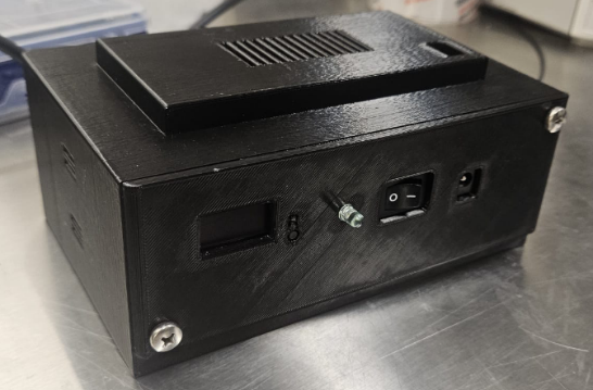
 Modular detector units: 3D-printed, stackable, one channel each (Fig. 1).
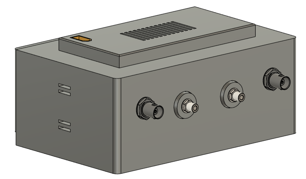
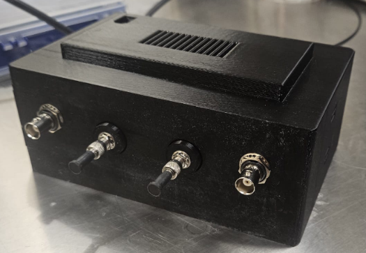 Detector front view (Fig. 2).
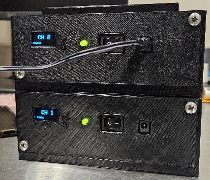
 Detector back view (Fig. 3).
Firmware
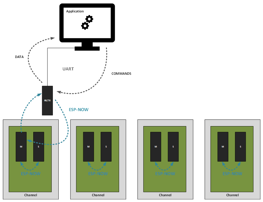 Firmware system: each channel is a Leader/Follower ESP32 pair on ESP-NOW; the RX/TX module bridges all channels to the host over UART.
 Sampling and summation in the INTEGRATE state.
State machines
I modeled both microcontrollers as state machines before writing any firmware.
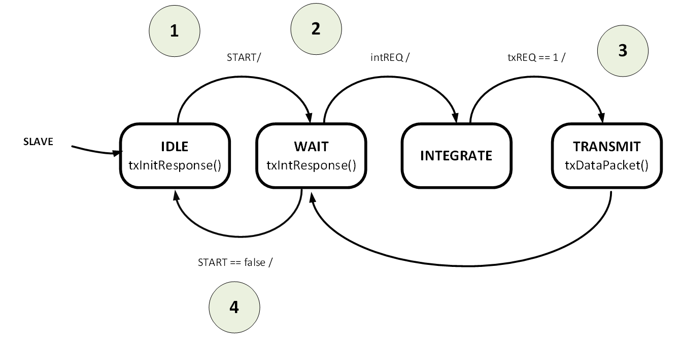 Follower: samples and integrates from its own ADC, then transmits the sum to the Leader on request.
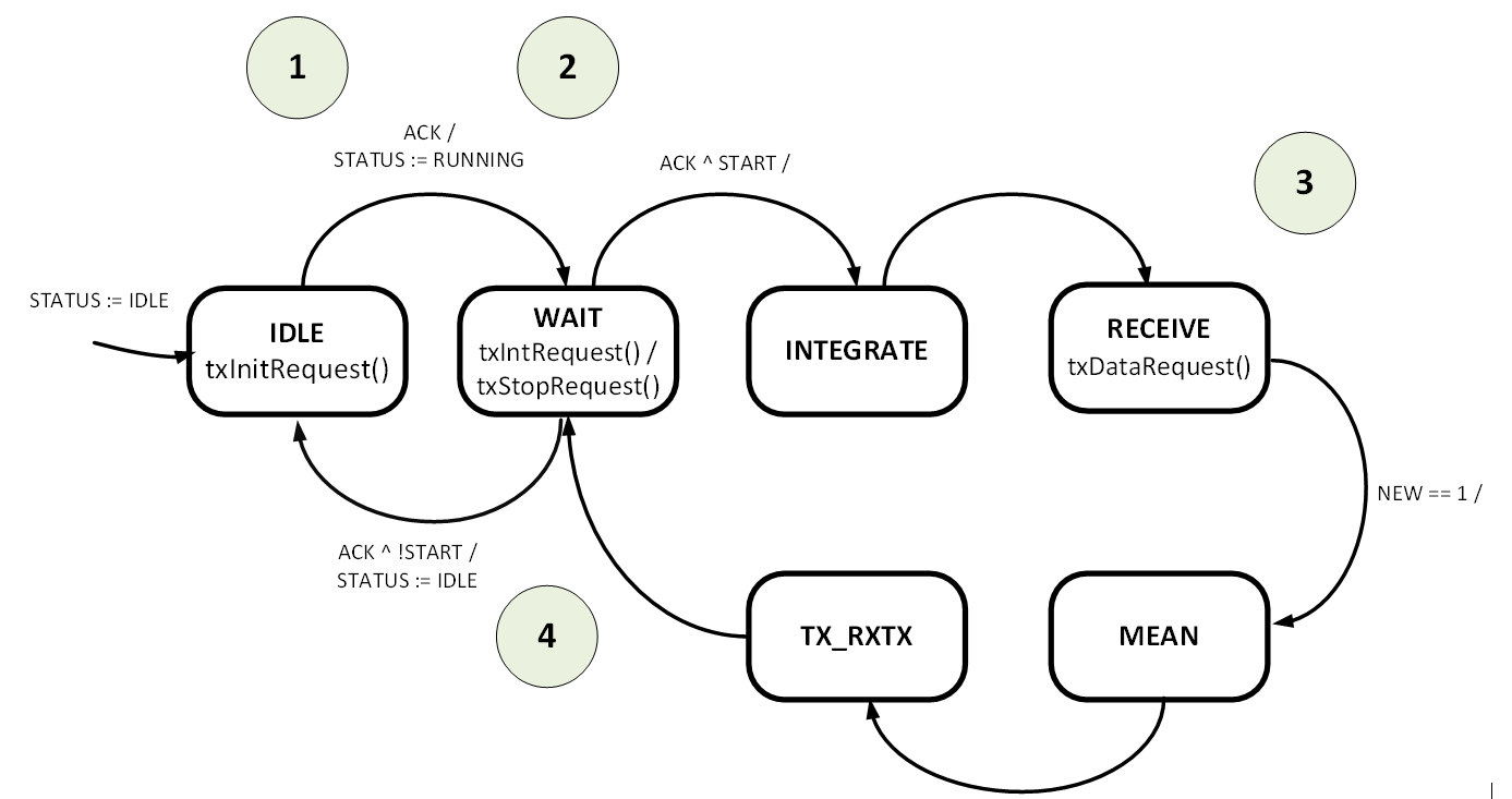 Leader: drives the Follower, computes the square-root-product mean of the two sums, and forwards the result to the RX/TX module.
Leader–Follower communication
The Leader and Follower exchange a small set of messages at each state transition over ESP-NOW.
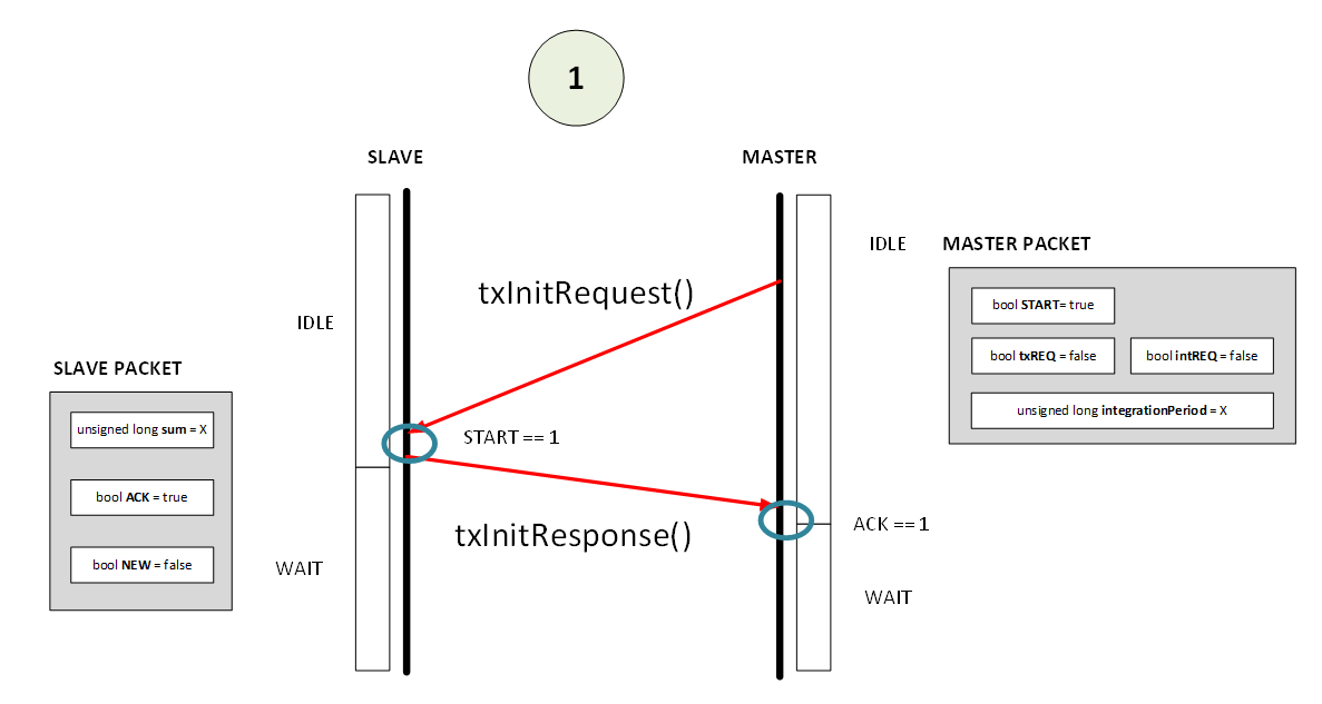 Initialization: the Leader requests, the Follower acknowledges, and both move to WAIT.
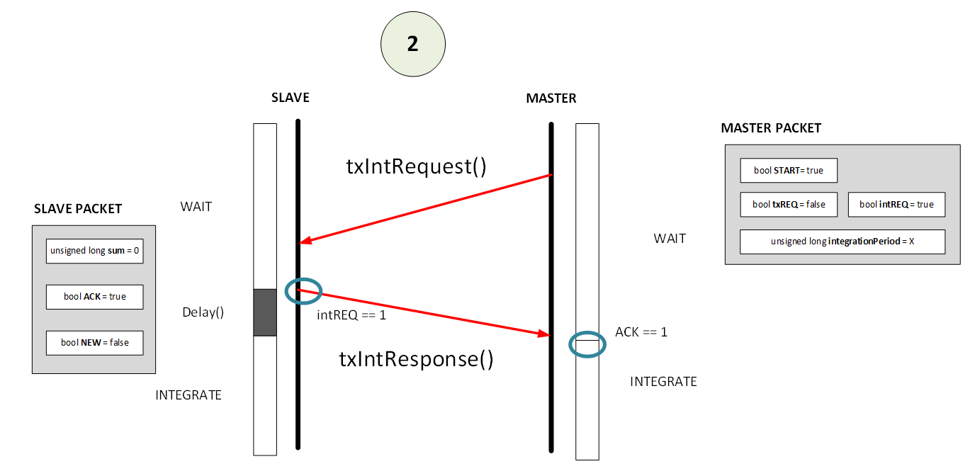 Integration: the pair synchronizes the start of each integration window.
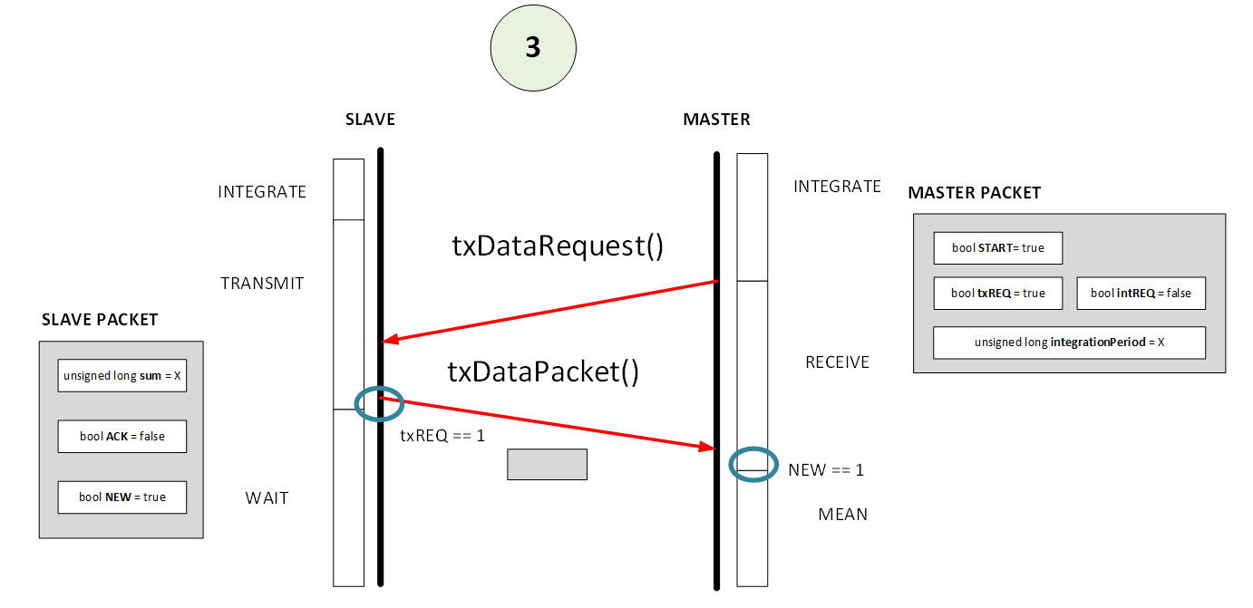 Transmission: the Follower sends its integrated sum to the Leader for the mean computation.
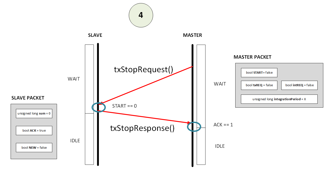 Termination: the Leader stops the channel and both devices return to IDLE.
Data path to the host
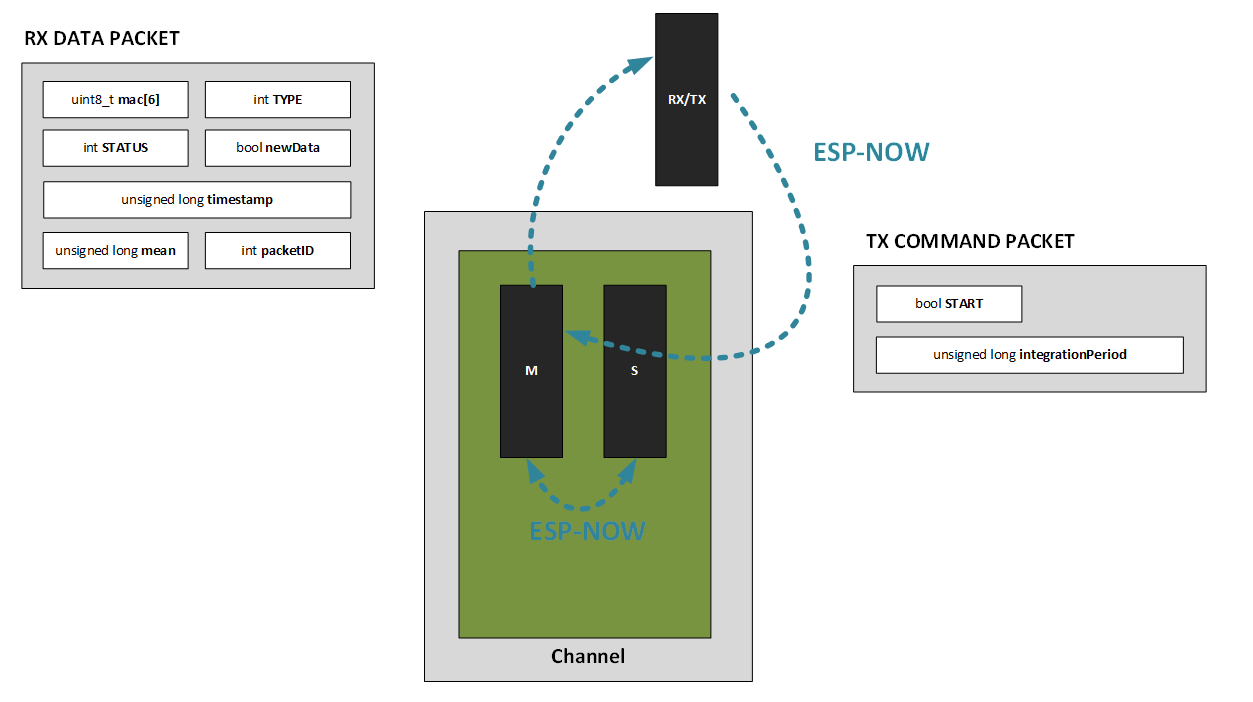 Leader ↔ RX/TX over ESP-NOW: data packets up, command packets down.
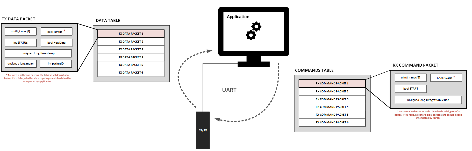 RX/TX ↔ application over UART: a DATA TABLE of all channels up, a COMMANDS TABLE down.
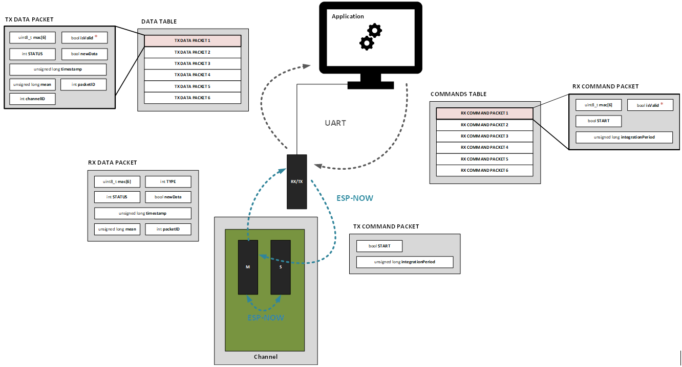 Full firmware overview: channels, RX/TX bridge, host, and every packet and table structure together.
Hardware: RX/TX module
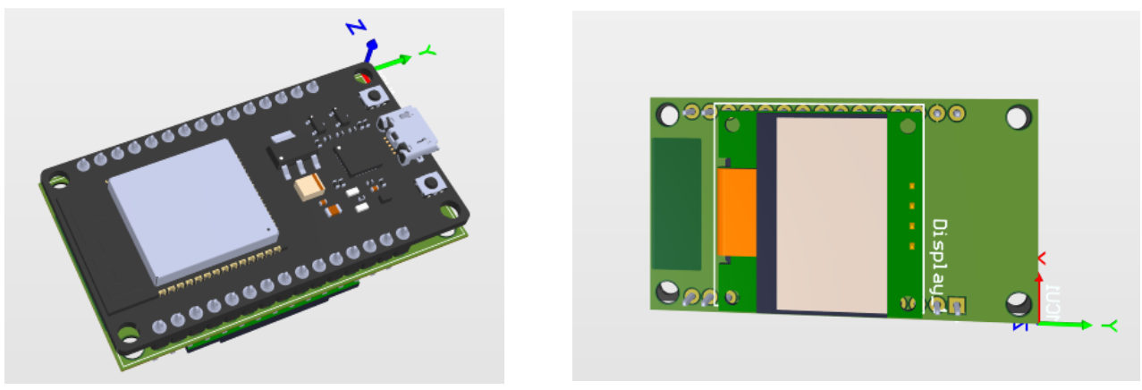 RX/TX module electronics: microcontroller and display boards (Fig. 9).
Hardware: Signal Acquisition Module (SiPM)
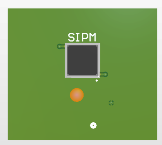 SiPM PCB, top (Fig. 11).
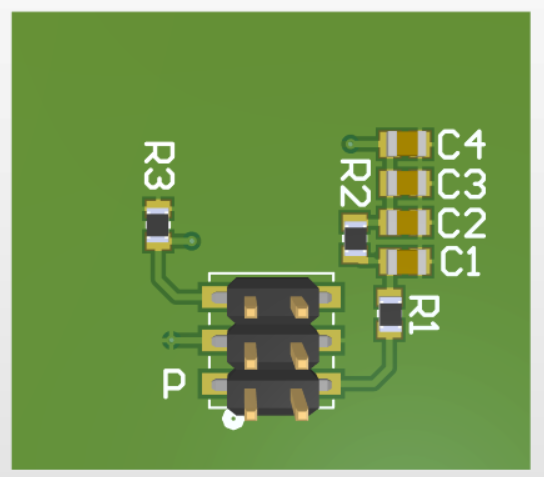 SiPM PCB, bottom: bias resistors, decoupling capacitors, connector (Fig. 11).
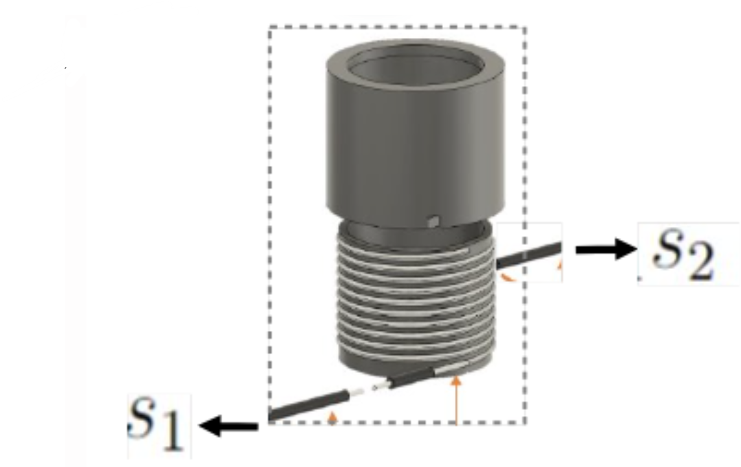
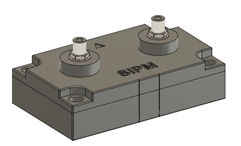 Signal Acquisition Module assembly, light-tight enclosure (Fig. 13).
Hardware: Detector module
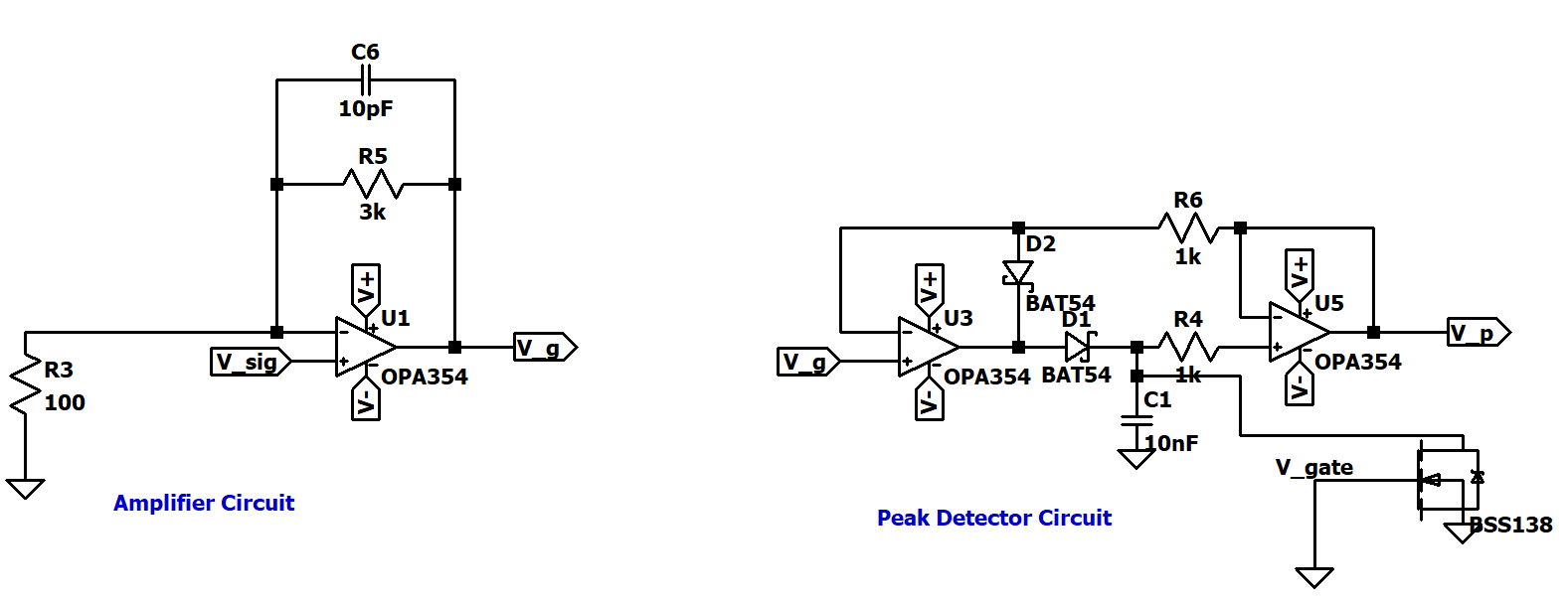 LTspice front-end schematic: amplifier and peak-detector stages, simulated before layout (Fig. 14).
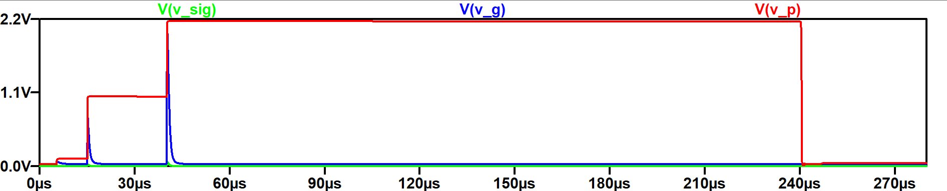 Simulated transient response of the signal (V_sig), gate (V_g), and peak (V_p) nodes (Fig. 14).
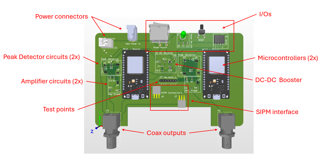 Main detector PCB, annotated: dual analog front ends, two microcontrollers, DC-DC booster, SiPM interface, coax outputs (Fig. 15).
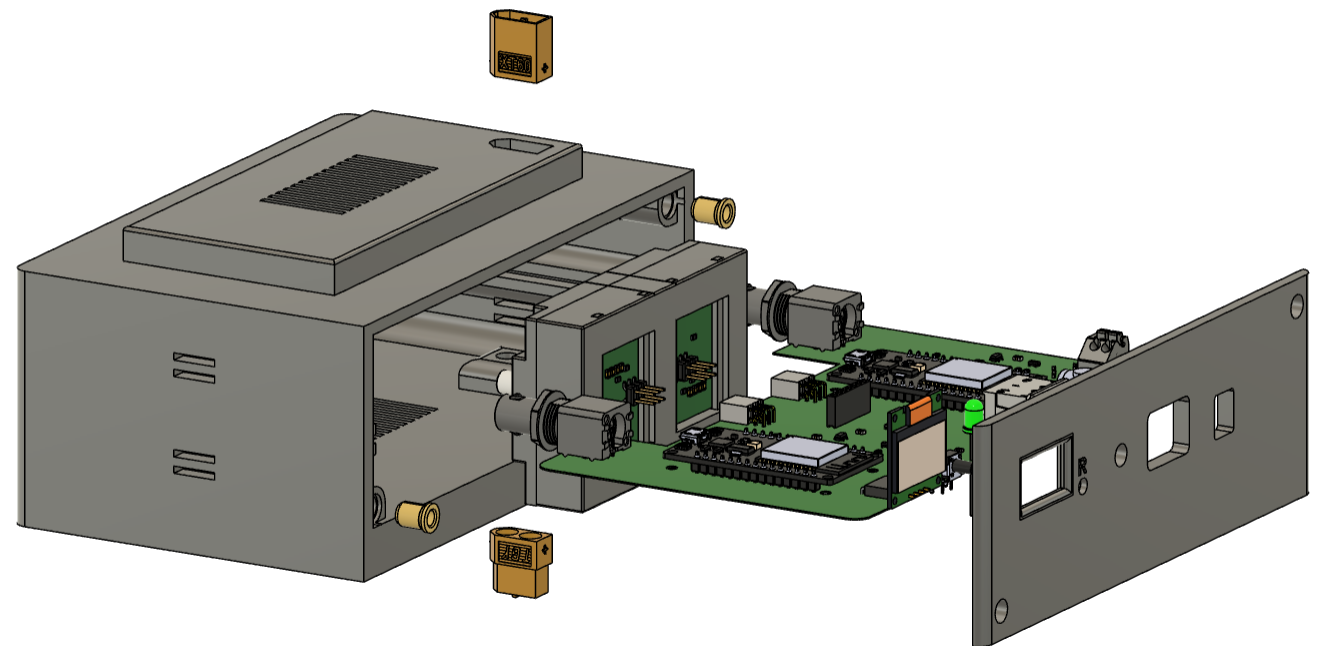 Detector module, exploded view (Fig. 16).
 Detector module, assembled (Fig. 16).
Modularity and results
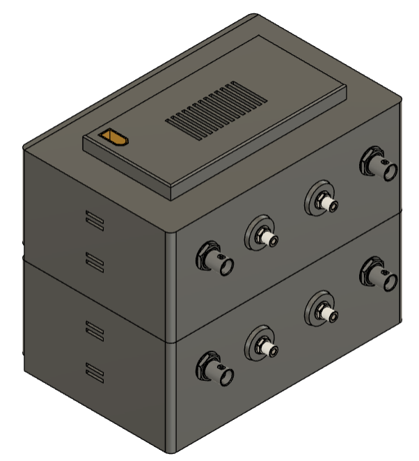 Modularity: units stack and share power through vertical connectors from one adapter (Fig. 17).
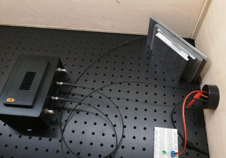 Experiment setup: optical-fiber input, lead wall, low-activity source (Fig. 18).
 Spiral fiber holder for the scintillating material (Fig. 19).
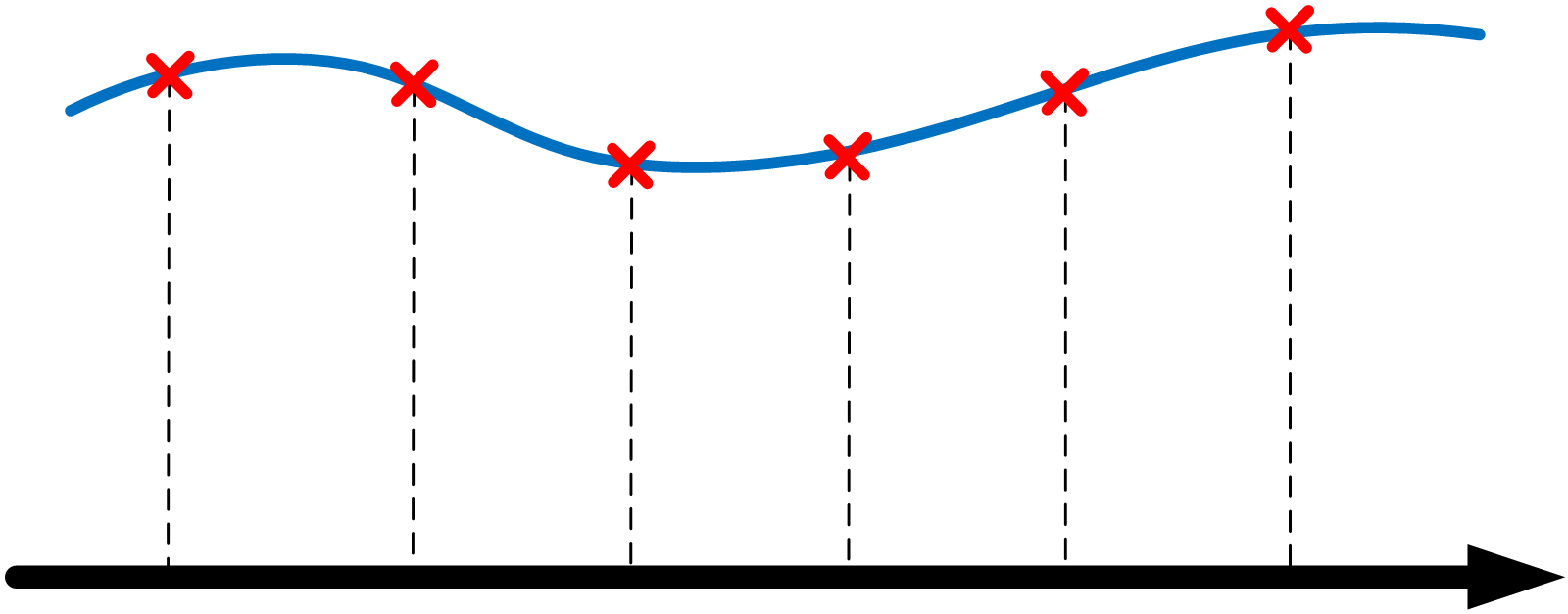
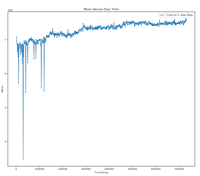 Measured raw data: mean channel value over time, largely constant for the low-activity source (Fig. 20).