Overview
A pipelined RISC-V processor implementing the RV32I base ISA, written in Verilog and pushed through synthesis and place-and-route in SkyWater 130nm. The core uses a three-stage pipeline: fetch (S1), decode/execute (S2), and memory/writeback (S3), fronted by direct-mapped instruction and data caches built on sky130 SRAM macros and connected to a 128-bit main-memory interface through an arbiter.
The three-stage organization is the deliberate middle ground for this target: deeper than a single-cycle core (so it can close timing at the course’s clock constraint) but shallow enough that the only hazard machinery needed is a single forwarding path and memory stalls, rather than a full multi-stage hazard unit.
What I did
- Pipeline datapath: partitioned the datapath into three stages with explicit pipeline registers (PC, instruction, ALU result, store data) carrying state from S1 → S2 → S3.
- Control path: built out the decode logic as separate, testable decoders: ALU-op, immediate, branch, memory, CSR, register-write, PC-select, and a dedicated forwarding decoder.
- Hazard resolution: implemented S3 → S2 forwarding for both ALU operands (
forward_a/forward_b) and store data (forward_data), withx0and write-enable guards so only genuine register-write instructions forward; multi-cycle memory accesses stall the pipeline via the cache/arbiter handshake. - Branch & jump: branch comparison (
BrEq/BrLT, signed or unsigned viaBrUn) is resolved in S2 and drives the PC-select mux, covering conditional branches,JAL, andJALRwith a low branch penalty. - ISA coverage: full RV32I (R/I-type arithmetic,
LOAD/STORE,BRANCH,LUI,AUIPC,JAL,JALR) plus the machine CSRs (tohost,hartid,status) needed by the test harness. - Memory system: direct-mapped I- and D-caches (a two-way set-associative variant is also implemented) over the banked sky130 SRAM macros.
- Physical implementation: drove synthesis (Genus) and place & route (Innovus) through Berkeley Hammer under a 9.0 ns clock constraint with explicit SRAM-macro placement, then ran Calibre DRC/LVS and Voltus power analysis. The block routed, but the layout did not close to a DRC-clean signoff (outstanding violations remained).
- Verification: ran the
riscv-testsassembly ISA suite and benchmarks (dhrystone, median, mm, multiply, qsort, rsort, spmv, towers, vvadd), plus directed ALU test-vector and PC testbenches.
Specs
| Item | Value |
|---|---|
| ISA | RV32I base + machine CSRs |
| Pipeline | 3 stages, IF / ID-EX / MEM-WB |
| Hazard handling | S3 → S2 forwarding (operands + store data); memory stalls |
| Branch resolution | In S2 (low branch penalty) |
| Caches | Direct-mapped I/D (two-way variant implemented), sky130 SRAM |
| Clock constraint | 9.0 ns (≈111 MHz target), sky130, 1.8 V |
| Flow | RTL → Genus (synth) → Innovus (P&R) → Calibre (DRC/LVS) |
| Verification | riscv-tests ISA suite + benchmark programs |
Approach and key decisions
Forwarding over stalling. With only three stages, the single read-after-write hazard worth optimizing is the producer-in-S3 / consumer-in-S2 case. A dedicated forwarding decoder handles it combinationally for ALU operands and store data, so back-to-back dependent instructions don’t bubble. The decoder explicitly excludes x0 and non-writing opcodes, which is the easy correctness trap in forwarding logic.
Branch resolution in S2. Resolving the branch condition and computing the target in the execute stage keeps the misprediction/redirect penalty to a single stage, which matters for the branch-heavy benchmarks in the test suite.
Caches and SRAM-macro placement. The most interesting physical-design wrinkle was the memory system: the direct-mapped caches map onto banked sky130 SRAM macros, which have to be explicitly floorplanned (placement constraints in the PAR config) rather than left to automatic placement, the same physical-design discipline a real block requires.
Figures
Microarchitecture
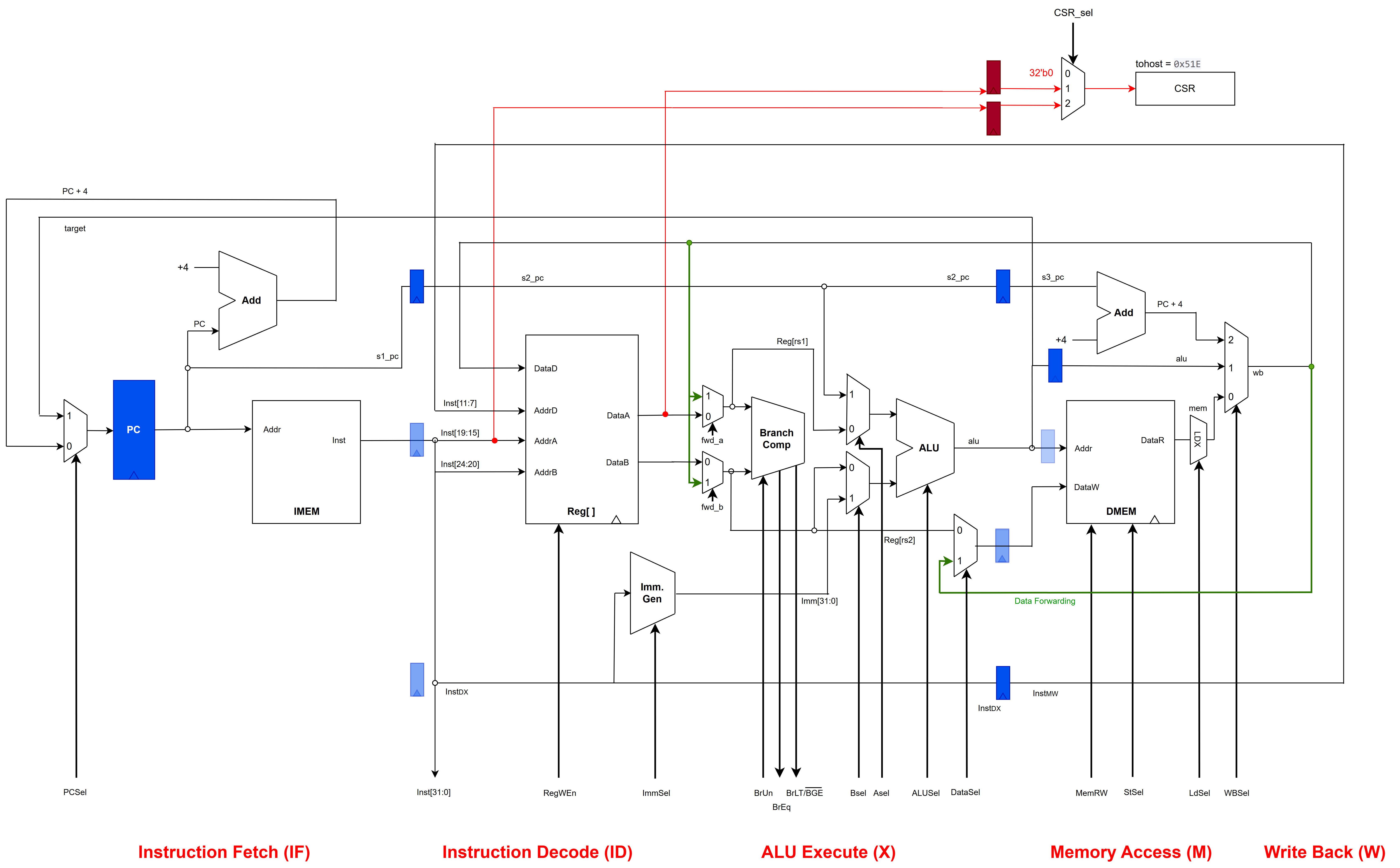 Full datapath across the IF, ID, ALU Execute, Memory, and Write Back stages, with pipeline registers (blue) and the data-forwarding paths (green).
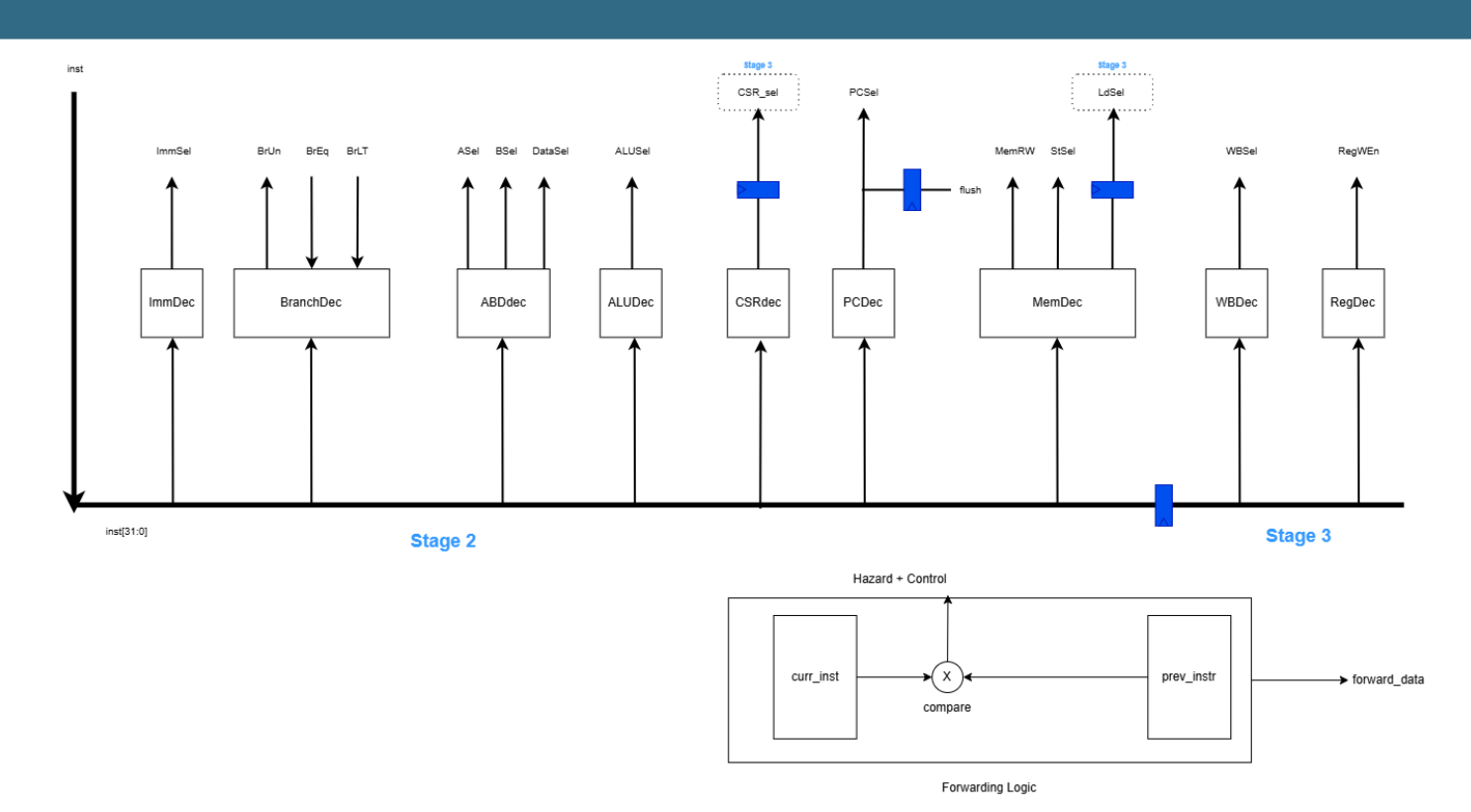 Control path: one decoder per signal group, split across Stage 2 and Stage 3, plus the forwarding-logic comparator that drives hazard control and data forwarding.
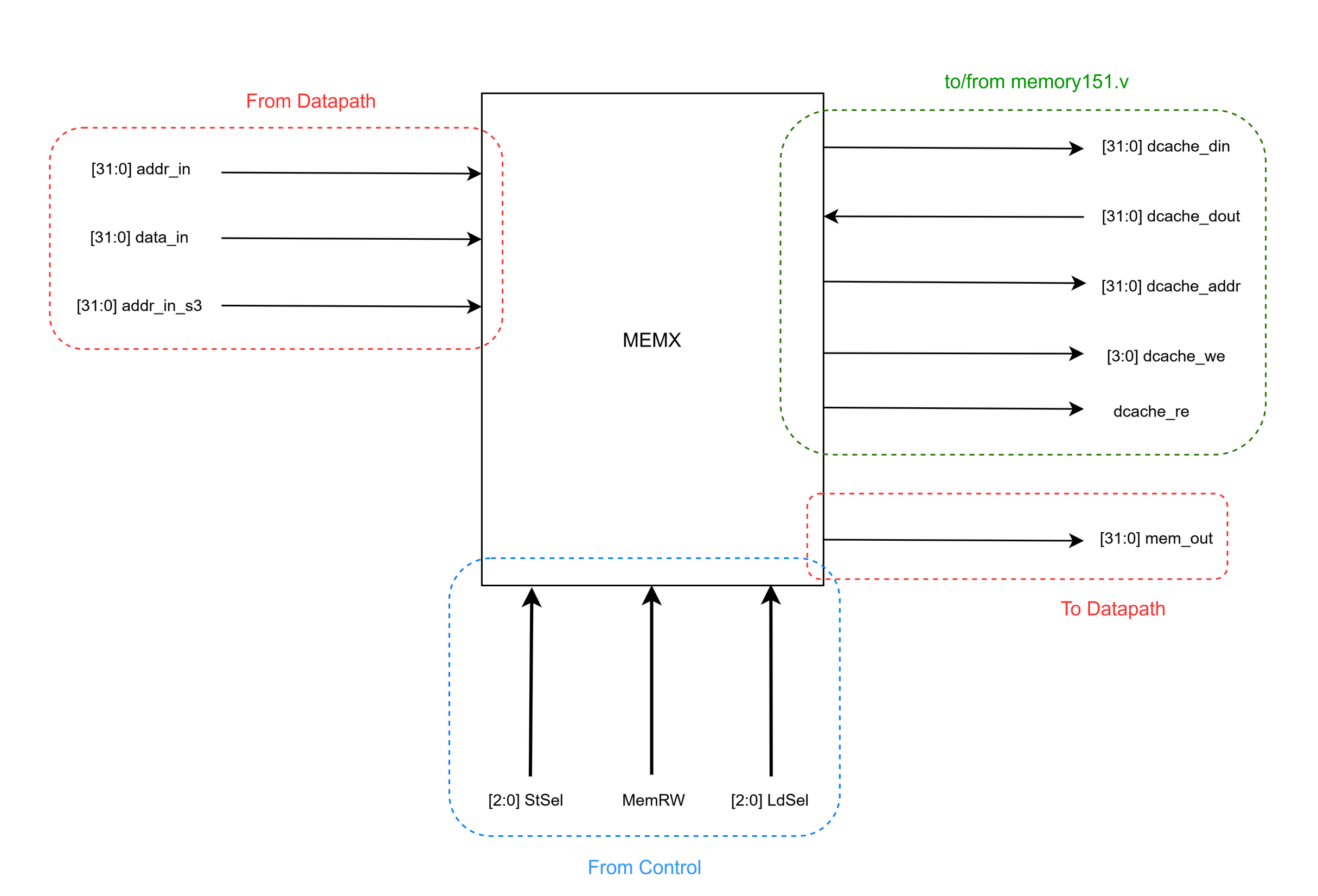 Memory-access stage (MEMX): the interface between the datapath, control, and the external memory model, feeding IMEM and DMEM.
Physical implementation
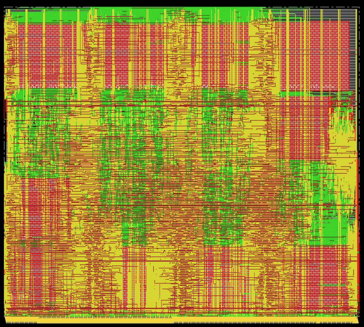 Post-place-and-route layout of the core in SkyWater 130nm (not DRC clean).