Overview
Designed and physically implemented the TX Digital front end of a 1000BASE-T Gigabit Ethernet PHY — the sub-module my 2-person subgroup owned within a complete PHY built by an 18-student EECS 251B class — following the IEEE 802.3 Clause 40 specification. The block accepts 8-bit transmit data from GMII at 125 MHz and produces a four-symbol 4D-PAM5 vector each clock cycle, feeding downstream FIR/DAC interface lanes.
The datapath consists of a 33-bit LFSR side-stream scrambler (with selectable MASTER/SLAVE polynomials), a convolutional trellis encoder, a 4D-PAM5 mapper, and four lanes of two-tap FIR filters driving thermometer-coded DAC outputs.
The source RTL lives in a private UC Berkeley course repository and can’t be shared publicly. The full report below covers the architecture, verification methodology, and physical-design results in detail; code samples are available on request.
What I did
- Scrambler RTL: SystemVerilog implementation of the 33-bit LFSR side-stream generator with master/slave tap polynomial selection, zero-seed lockup protection, and the auxiliary bit-generation logic that produces
Scn,Syn, andSgnfor downstream blocks. - 4D-PAM5 mapper RTL: Top-level mapper plus a separate
PAM5_LUTchild module covering all 13 IEEE-defined mapping modes, sign-reversal logic, andtx_enablememory. - Verification: Wrote a Python golden model derived directly from IEEE 802.3-2018 Tables 40-1 and 40-2 to generate expected outputs for the mapper. Built an exhaustive SystemVerilog testbench sweeping all 245,760 input combinations (2 sign states × 15 modes × 512
Sd_nvalues × 16Sg_nvalues) against the golden model. - Synthesis and place & route: Worked jointly on the physical implementation flow (Genus → Innovus → Pegasus) under an 8 ns clock constraint on a 180 µm × 180 µm floorplan.
Results
| Metric | Value |
|---|---|
| Clock target | 125 MHz (8 ns) |
| Setup slack | +0.072 ns (post-route, ss corner) |
| Hold slack | +0.091 ns (post-route, ff corner) |
| Total power | 3.108 mW (TT, 25°C, 1.8V) |
| Std-cell area | 18,497 µm² |
| Placement density | 69.96% |
| Physical checks | DRC / LVS / DRV clean |
| Mapper verification | 245,760 input combinations vs. Python golden model |
Approach and key decisions
Verification strategy. Rather than rely on directed mapper tests, I built a Python golden model directly from the IEEE tables and used it to generate exhaustive stimulus. This caught corner-case mode and sign-reversal interactions that directed tests would have missed, and made regression on any RTL change trivial.
Zero-seed lockup. The LFSR can stuck at all-zero if seeded that way; the RTL explicitly checks LFSR_seed == 0 and substitutes 33'h1. Small detail, but it’s the kind of standards-compliance trap that fails silently in simulation.
Block partitioning of the mapper. Splitting the mapper into a pure-combinational PAM5_LUT child and a wrapper handling sign-randomization and tx_enable memory kept the LUT independently verifiable against the IEEE tables, and isolated the wrapper logic for separate testing.
Figures
Architecture and RTL
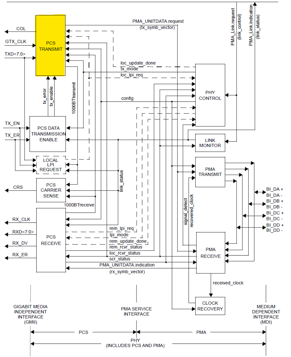 The PCS within the 1000BASE-T PHY, with the implemented TX Digital path highlighted (report Fig. 1).
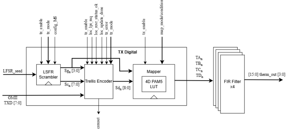 TX Digital datapath: scrambler, encoder, 4D-PAM5 mapper, then 4× two-tap FIR lanes (report Fig. 2).
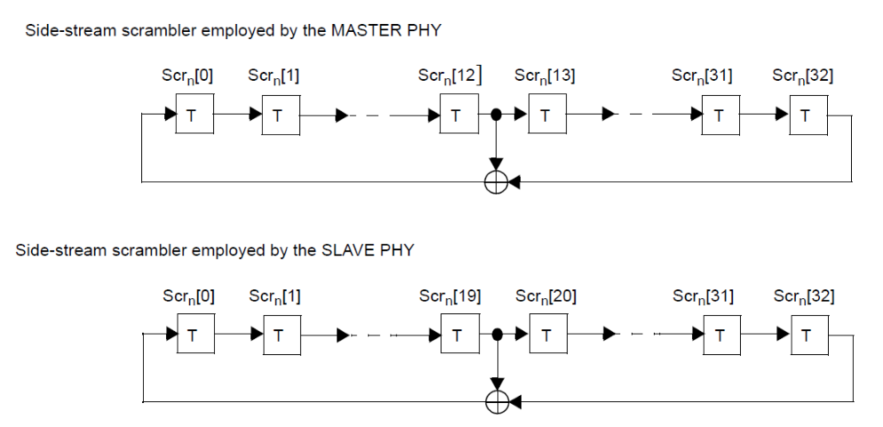 33-bit side-stream scrambler LFSR, with the MASTER and SLAVE feedback-tap polynomials (report Fig. 3).
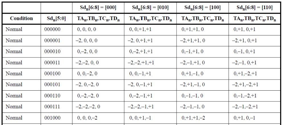 4D-PAM5 bit-to-symbol mapping, even subsets (report Fig. 4, IEEE Table 40-1).
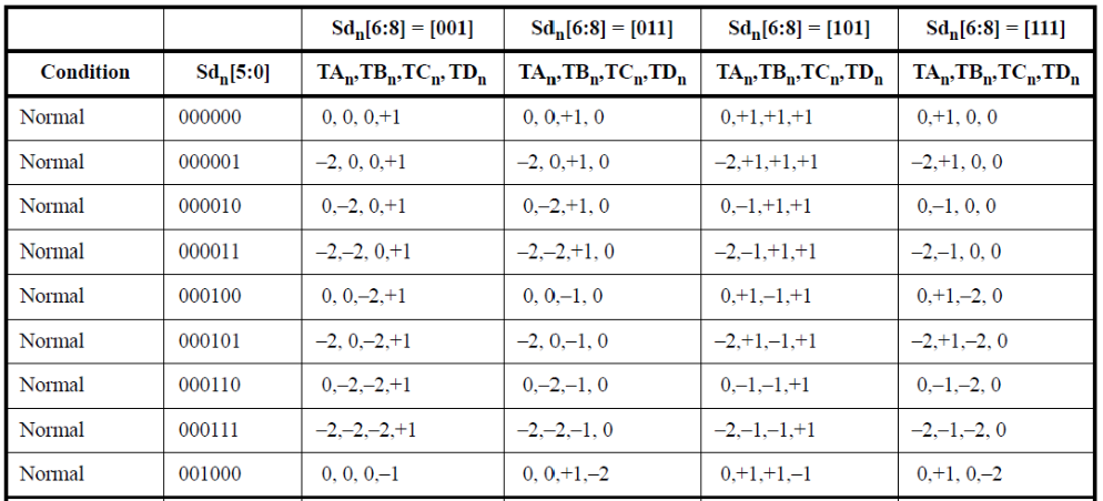 4D-PAM5 bit-to-symbol mapping, odd subsets (report Fig. 5, IEEE Table 40-2).
Physical design
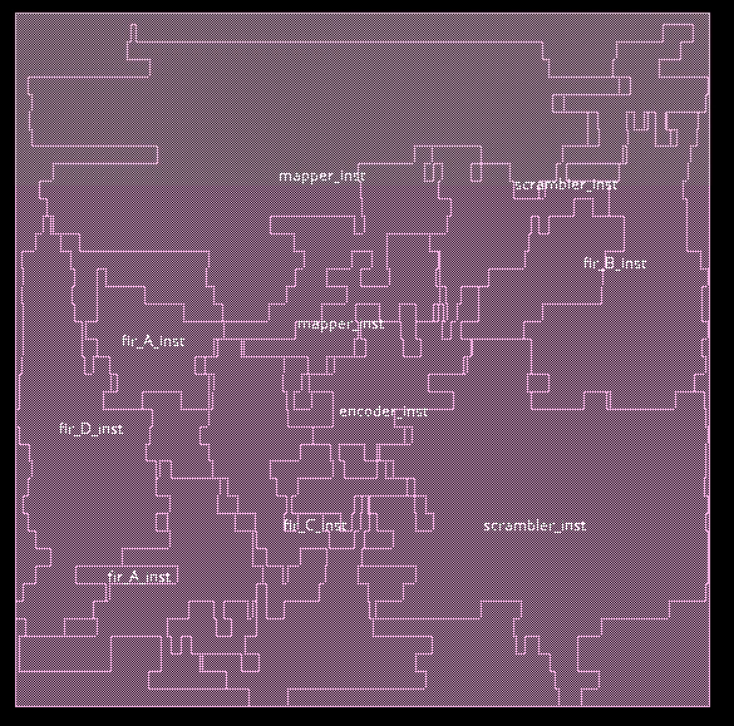 Post-placement view of the tx_digital block, with the scrambler, mapper, encoder, and FIR lanes labeled (report Fig. 6).
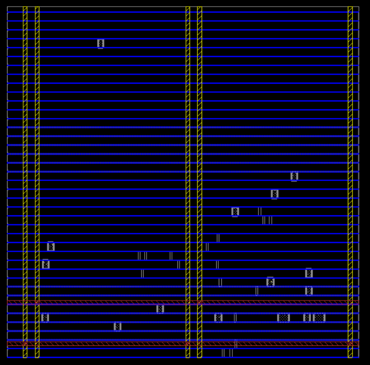 Floorplan of the 180 µm × 180 µm die at 69.96% placement density (report Fig. 7).
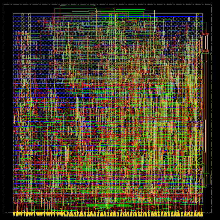 Full routed layout of the tx_digital block (report Fig. 8).
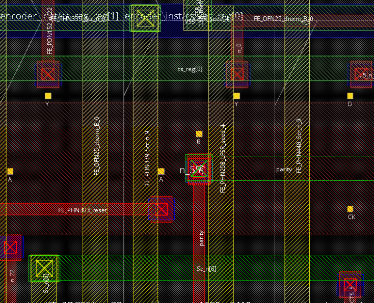 Zoomed routing detail after place-and-route (report Fig. 9).