Overview
Design, simulation, and validation of a general-purpose operational amplifier built entirely from discrete bipolar transistors. The amplifier is organized as three cascaded stages, a differential-amplifier input, a buffer, and a Class-AB output stage, sized from hand calculations, refined in LTspice, then prototyped and characterized on a breadboard.
What I did
- Topology: designed three separate stages: a differential amplifier, a buffer, and an output stage.
- Hand analysis first: determined the circuit parameters by hand to meet the design requirements before touching a simulator.
- Simulation: modeled the full amplifier in LTspice and adjusted component values as needed to hit the targets.
- Stage-by-stage validation: built each stage on a breadboard and validated it independently with an oscilloscope and spectrum analyzer before integrating.
- Integration & test: combined the stages, measured the open-loop properties, then tested the amplifier in a closed-loop non-inverting configuration. Potentiometers at R8, R13, and R16 allowed fine-tuning of the bias and gain.
Results
| Measurement | Result |
|---|---|
| Open-loop gain | 2500 V/V: 5 Vpp out from 2 mVpp in |
| Closed-loop gain (non-inv.) | 150 V/V: 3 Vpp out from 10 mVpp in |
| Voltage transfer char. | Measured across the closed-loop system |
| Frequency response | Measured on the closed-loop system |
Approach and key decisions
Why breadboard validation matters. Building on a breadboard comes with challenges, parasitic capacitance chief among them, but for smaller analog signals it’s a valuable step: every node is probeable and any component can be swapped in seconds, which makes validation far easier than on an integrated circuit.
The lesson from cascading. Each stage worked in isolation, but when I cascaded them the output deviated from the expected result. The cause was non-ideal inter-stage loading, a reminder that stage output/input impedances have to be designed for the actual neighboring stage, not an ideal one. Adjusting for loading brought the combined amplifier back in line.
Figures
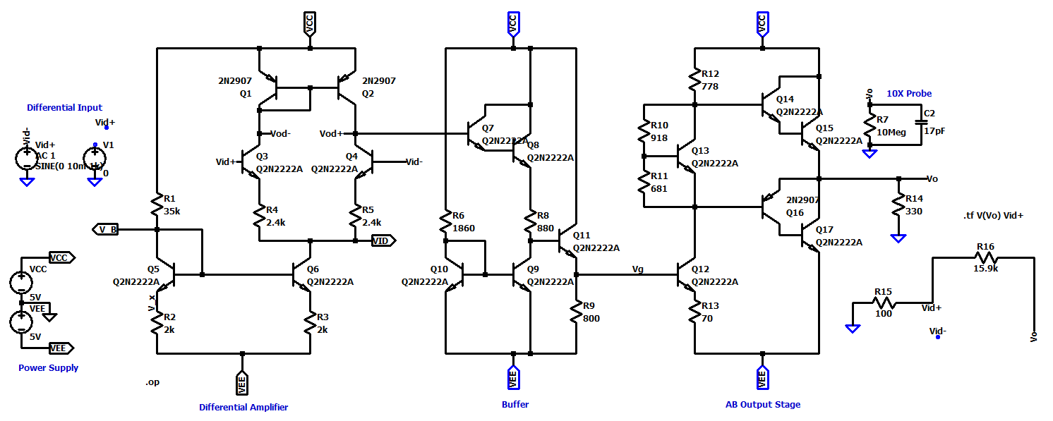 Full LTspice schematic, differential amplifier → buffer → AB output stage (Fig. 21).
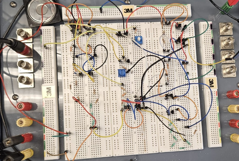 Breadboard prototype of the non-inverting configuration (Fig. 22).
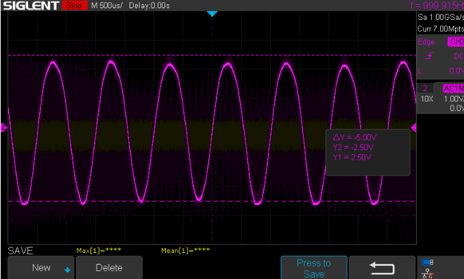 (A) Open-loop response: 2500 V/V gain, 5 Vpp out from 2 mVpp in (Fig. 23).
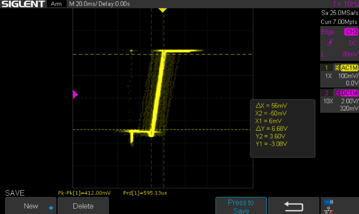
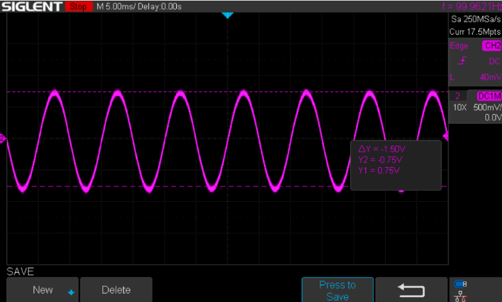 (B) Closed-loop non-inverting response: 150 V/V gain, 3 Vpp out from 10 mVpp in (Fig. 24).
 (C) Voltage transfer characteristic of the closed-loop system (Fig. 25).
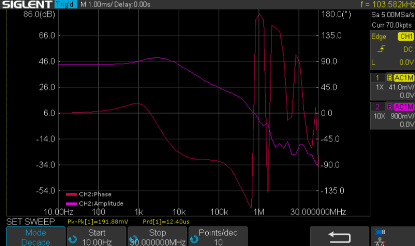 (D) Closed-loop frequency response, magnitude and phase (Fig. 26).